VIPer20/SP/DIP - VIPer20A/ASP/ADIP
TRANSCONDUCTANCE ERROR AMPLIFIER
achieve different compensation laws. A capacitor
will provide an integrator function, thus eliminating
the DC static error, and a resistance in series
leads to a flat gain at higher frequency, insuring a
correct phase margin. This configuration is
illustrated in figure 18.
The VIPer20/20A includes a transconductance
error amplifier. Transconductance Gm is the
change in output current (I
) versus change in
COMP
input voltage (V ). Thus:
DD
∂I
COMP
------------------------
G
=
m
∂V
As shown in figure 18 an additional noise filtering
capacitor of 2.2 nF is generally needed to avoid
any high frequency interference.
DD
The output impedance Z
at the output of this
COMP
amplifier (COMP pin) can be defined as:
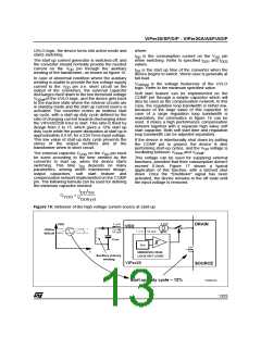
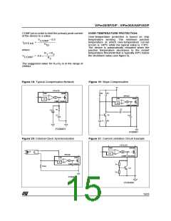
It can also be interesting to implement a slope
compensation when working in continuous mode
with duty cycle higher than 50%. Figure 19 shows
such a configuration. Note that R1 and C2 build
the classical compensation network, and Q1 is
injecting the slope compensation with the correct
polarity from the oscillator sawtooth.
∂V
∂ V
1
COMP
COMP
--------------------------
-------- --------------------------
Z
=
=
×
COMP
G
∂V
∂I
COMP
DD
m
This last equation shows that the open loop gain
A
can be related to G and Z
:
VOL
m
COMP
A
= G x Z
VOL
m
COMP
EXTERNAL CLOCK SYNCHRONIZATION
where G value for VIPer50/50A is 1.5 mA/V
typically.
m
The OSC pin provides
a
synchronisation
capability, when connected to an external
frequency source. Figure 20 shows one possible
schematic to be adapted depending on the
specific needs. If the proposed schematic is used,
the pulse duration must be kept at a low value
(500ns is sufficient) for minimizing consumption.
The optocoupler must be able to provide 20mA
through the optotransistor.
G is well defined by specification, but Z
and
COMP
m
therefore A
are subject to large tolerances. An
VOL
impedance Z can be connected between the
COMP pin and ground in order to define more
accurately the transfer function F of the error
amplifier, according to the following equation, very
similar to the one above:
F
= Gm x Z(S)
(S)
The error amplifier frequency response is reported
in figure 10 for different values of a simple
resistance connected on the COMP pin. The
unloaded transconductance error amplifier shows
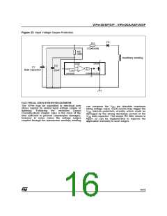
PRIMARY PEAK CURRENT LIMITATION
The primary I
current and, as resulting
DPEAK
effect, the output power can be limited using the
simple circuit shown in figure 21. The circuit based
on Q1, R and R clamps the voltage on the
an internal Z
of about 330 KΩ. More complex
COMP
impedance can be connected on the COMP pin to
1
2
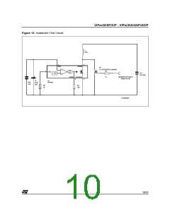
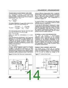
Figure 16: Mixed Soft Start and Compensation
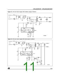
Figure 17: Latched Shut Down
D2
D3
VIPer20
VIPer20
R1
VDD
DRAIN
VDD
DRAIN
-
Q2
-
OSC
R3
R2
OSC
13V
+
13V
+
COMP SOURCE
D1
COMP SOURCE
AUXILIARY
WINDING
R3
R2
Q1
C4
R1
R4
C3
C2
+
+
C1
Shutdown
D1
FC00431
FC00440
14/25

 STMICROELECTRONICS [ ST ]