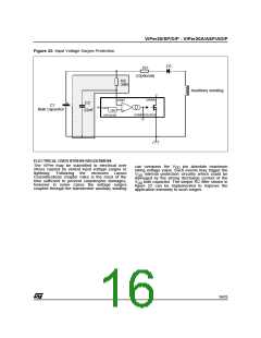
VIPer20/SP/DIP - VIPer20A/ASP/ADIP
OPERATION DESCRIPTION:
CURRENT MODE TOPOLOGY
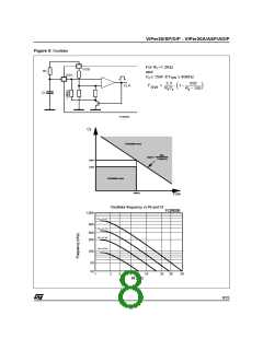
F
is the normal switching frequency.
SW
I
is the minimum controllable current,
STBY
corresponding to the minimum on time that the
device is able to provide in normal operation. This
current can be computed as:
The current mode control method, like the one
integrated in the VIPer20/20A uses two control
loops - an inner current control loop and an outer
loop for voltage control. When the Power
MOSFET output transistor is on, the inductor
current (primary side of the transformer) is
monitored with a SenseFET technique and
(t + t )V
b
d
IN
--------------------------------
I
=
STBY
L
P
t + t is the sum of the blanking time and of the
b
d
propagation time of the internal current sense and
comparator, and roughly represents the minimum
converted into a voltage V proportional to this
S
current. When V reaches V
(the amplified
on time of the device. Note that P
may be
S
COMP
STBY
output voltage error) the power switch is switched
off. Thus, the outer voltage control loop defines
the level at which the inner loop regulates peak
current through the power switch and the primary
winding of the transformer.
affected by the efficiency of the converter at low
load, and must include the power drawn on the
primary auxiliary voltage.
As soon as the power goes below this limit, the
auxiliary secondary voltage starts to increase
above the 13V regulation level forcing the output
voltage of the transconductance amplifier to low
Excellent D.C. open loop and dynamic line
regulation is ensured due to the inherent input
voltage feedforward characteristic of the current
mode control. This results in an improved line
regulation, instantaneous correction to line
changes and better stability for the voltage
regulation loop.
state (V
< V
). This situation leads to
COMP
COMPth
the shutdown mode where the power switch is
maintained in the off state, resulting in missing
cycles and zero duty cycle. As soon as V gets
DD
COMPth
back to the regulation level and the V
threshold is reached, the device operates again.
The above cycle repeats itself indefinitely,
providing a burst mode of which the effective duty
cycle is much lower than the minimum one when in
normal operation. The equivalent switching
frequency is also lower than the normal one,
leading to a reduced consumption on the input
mains lines. This mode of operation allows the
VIPer20/20A to meet the new German "Blue
Angel" Norm with less than 1W total power
consumption for the system when working in
stand-by. The output voltage remains regulated
around the normal level, with a low frequency
ripple corresponding to the burst mode. The
amplitude of this ripple is low, because of the
output capacitors and because of the low output
current drawn in such conditions. The normal
operation resumes automatically when the power
Current mode topology also ensures good
limitation in the case of short circuit. During the
first phase the output current increases slowly
following the dynamic of the regulation loop. Then
it reaches the maximum limitation current
internally set and finally stops because the power
supply on V
is no longer correct. For specific
DD
applications the maximum peak current internally
set can be overridden by limiting the voltage
excursion externally on the COMP pin. An
integrated blanking filter inhibits the PWM
comparator output for a short time after the
integrated Power MOSFET is switched on. This
function prevents anomalous or premature
termination of the switching pulse in the case of
current spikes caused by primary side capacitance
or secondary side rectifier reverse recovery time.
gets back levels which are higher than P
.
STBY
STAND-BY MODE
Stand-by operation in nearly open load condition
automatically leads to a burst mode operation
allowing voltage regulation on the secondary side.
The transition from normal operation to burst
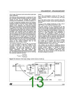
HIGH
SOURCE
VOLTAGE
START-UP
CURRENT
An integrated high voltage current source provides
a bias current from the DRAIN pin during the start-
up phase. This current is partially absorbed by
internal control circuits which are placed into a
standby mode with reduced consumption and are
also provided to the external capacitor connected
mode operation happens for a power P
by:
given
STBY
2
1
2
--
P
=
L I
F
STBY
STBY
Where:
L is the primary inductance of the transformer.
P
SW
to the V
pin. As soon as the voltage on this pin
DD
reaches the high voltage threshold V
of the
DDon
P
12/25

 STMICROELECTRONICS [ ST ]