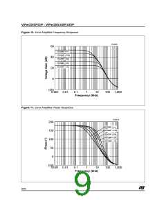
VIPer20/SP/DIP - VIPer20A/ASP/ADIP
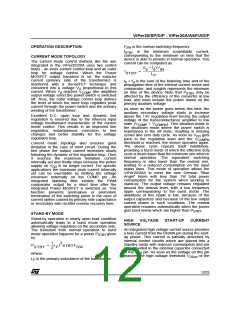
UVLO logic, the device turns into active mode and
starts switching.
where:
is the consumption current on the V
I
pin
DD2
DD
DD
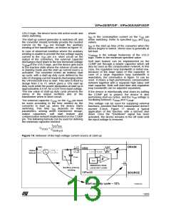
The start up current generator is switched off, and
the converter should normally provide the needed
when switching. Refer to specified I
values.
and I
DD1
current on the V
pin through the auxiliary
DD
t
is the start up time of the converter when the
SS
winding of the transformer, as shown on figure 15.
device begins to switch. Worst case is generally at
full load.
In case of abnormal condition where the auxiliary
winding is unable to provide the low voltage supply
V
is the voltage hysteresis of the UVLO
DDhyst
current to the V
pin (i.e. short circuit on the
DD
logic. Refer to the minimum specified value.
output of the converter), the external capacitor
discharges itself down to the low threshold voltage
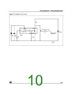
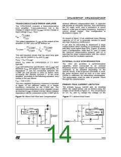
Soft start feature can be implemented on the
COMP pin through a simple capacitor which will
also be used as the compensation network. In this
case, the regulation loop bandwidth is rather low,
because of the large value of this capacitor. In
case of a large regulation loop bandwidth is
mandatory, the schematics in figure 16 can be
used. It mixes a high performance compensation
network together with a separate high value soft
start capacitor. Both soft start time and regulation
loop bandwidth can be adjusted separately.
V
of the UVLO logic, and the device gets back
DDoff
to the inactive state where the internal circuits are
in standby mode and the start up current source is
activated. The converter enters an endless start
up cycle, with a start-up duty cycle defined by the
ratio of charging current towards discharging when
the VIPer20/20A tries to start. This ratio is fixed by
design from 2 to 15, which gives a 12% start up
duty cycle while the power dissipation at start up is
approximately 0.6 W, for a 230 Vrms input voltage.
This low value of start-up duty cycle prevents the
stress of the output rectifiers and of the
transformer when in short circuit.
If the device is intentionally shut down by putting
the COMP pin to ground, the device is also
performing start-up cycles, and the V voltage is
DD
.
oscillating between V
and V
DDon
DDoff
The external capacitor C
on the V pin must
DD
VDD
be sized according to the time needed by the
converter to start up, when the device starts
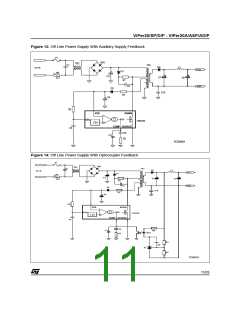
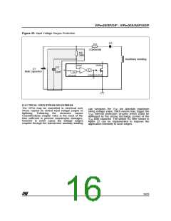
This voltage can be used for supplying external
functions, provided that their consumption doesn’t
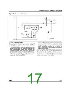
exceed 0.5mA. Figure 17 shows a typical
application of this function, with a latched shut
down. Once the "Shutdown" signal has been
activated, the device remains in the off state until
the input voltage is removed.
switching. This time t
depends on many
SS
parameters, among which transformer design,
output capacitors, soft start feature and
compensation network implemented on the COMP
pin. The following formula can be used for defining
the minimum capacitor needed:
I
t
DD SS
-------------------------
C
>
VDD
V
DDhyst
Figure 15: Behavior of the high voltage current source at start-up
3 mA
VDD
2 mA
15 mA
CVDD
DRAIN
VDD
VDDon
VDDoff
1 mA 15 mA
Ref.
t
UNDERVOLTAGE
LOCK OUT LOGIC
Auxiliary primary
winding
VIPer20
SOURCE
Start up duty cycle ~ 12%
FC00101A
13/25

 STMICROELECTRONICS [ ST ]