VIPer12ADIP / VIPer12AS
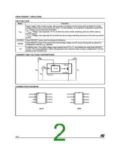
PIN FUNCTION
Name
Function
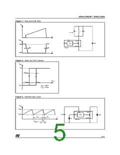
Power supply of the control circuits. Also provides a charging current during start up thanks to a high
voltage current source connected to the drain. For this purpose, an hysteresis comparator monitors the
V
voltage and provides two thresholds:
DD
V
- V
: Voltage value (typically 14.5V) at which the device starts switching and turns off the start up
DDon
DD
current source.
- V : Voltage value (typically 8V) at which the device stops switching and turns on the start up current
DDoff
source.
SOURCE Power MOSFET source and circuit ground reference.
Power MOSFET drain. Also used by the internal high voltage current source during start up phase for
DRAIN
charging the external V capacitor.
DD
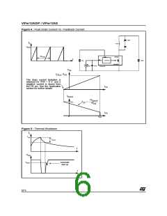
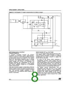
Feedback input. The useful voltage range extends from 0V to 1V, and defines the peak drain MOSFET
current. The current limitation, which corresponds to the maximum drain current, is obtained for a FB pin
shorted to the SOURCE pin.
FB
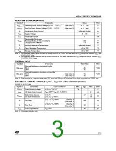
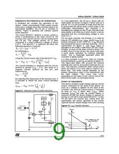
CURRENT AND VOLTAGE CONVENTIONS
IDD
ID
VDD
DRAIN
IFB
FB
CONTROL
VDD
VD
SOURCE
VFB
VIPer12A
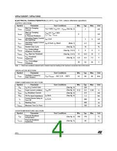
CONNECTION DIAGRAM
1
2
8
7
1
8
7
6
5
DRAIN
DRAIN
DRAIN
DRAIN
SOURCE
DRAIN
DRAIN
DRAIN
DRAIN
SOURCE
2
SOURCE
SOURCE
FB
3
3
4
6
5
FB
4
VDD
VDD
SO-8
DIP8
2/15

 STMICROELECTRONICS [ ST ]