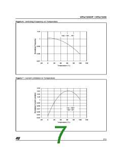
VIPer12ADIP / VIPer12AS
FEEDBACK PIN PRINCIPLE OF OPERATION
In a real application, the FB pin is driven with an
optocoupler as shown on figure 9 which acts as a
pull up. So, it is not possible to really short this pin
to ground and the above drain current value is not
achievable. Nevertheless, the capacitor C is
averaging the voltage on the FB pin, and when the
optocoupler is off (start up or short circuit), it can be
assumed that the corresponding voltage is very
close to 0 V.
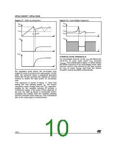
For low drain currents, the formula (1) is valid as
long as IFB satisfies IFB< IFBsd, where IFBsd is an
internal threshold of the VIPer12A. If IFB exceeds
this threshold the device will stop switching. This is
represented on figure 4, and IFBsd value is
specified in the PWM COMPARATOR SECTION.
Actually, as soon as the drain current is about 12%
of Idlim, that is to say 50 mA, the device will enter
a burst mode operation by missing switching
cycles. This is especially important when the
converter is lightly loaded.
It is then possible to build the total DC transfer
function between ID and IFB as shown on figure 10.
This figure also takes into account the internal
blanking time and its associated minimum turn on
time. This imposes a minimum drain current under
which the device is no more able to control it in a
linear way. This drain current depends on the
primary inductance value of the transformer and
the input voltage. Two cases may occur,
depending on the value of this current versus the
fixed 50 mA value, as described above.
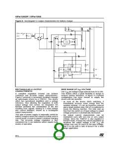
A feedback pin controls the operation of the
device. Unlike conventional PWM control circuits
which use a voltage input (the inverted input of an
operational amplifier), the FB pin is sensitive to
current. Figure 9 presents the internal current
mode structure.
The Power MOSFET delivers a sense current Is
which is proportional to the main current Id. R2
receives this current and the current coming from
the FB pin. The voltage across R2 is then
compared to a fixed reference voltage of about
0.23 V. The MOSFET is switched off when the
following equation is reached:
R2 (IS + IFB) = 0.23V
By extracting IS:
0.23V
IS = ------------- – I FB
R2
Using the current sense ratio of the MOSFET GID
0.23V
ID = GID IS = GID ------------- – I FB
R2
:
The current limitation is obtained with the FB pin
shorted to ground (VFB = 0 V). This leads to a
negative current sourced by this pin, and
expressed by:
0.23V
IFB = – -------------
R1
By reporting this expression in the previous one, it
is possible to obtain the drain current limitation
START UP SEQUENCE
IDlim
:
This device includes a high voltage start up current
source connected on the drain of the device. As
soon as a voltage is applied on the input of the
converter, this start up current source is activated
as long as VDD is lower than VDDon. When
reaching VDDon, the start up current source is
switched off and the device begins to operate by
turning on and off its main power MOSFET. As the
FB pin does not receive any current from the
optocoupler, the device operates at full current
capacity and the output voltage rises until reaching
1
1
IDlim = GID 0.23V ----- + -----
R2 R 1
Figure 9 : Internal Current Control Structure
DRAIN
60kHz
OSCILLATOR
Id
+Vdd
S
PWM
LATCH
Q
R
Figure 10 : IFB Transfer function
Secondary
feedback
I
Dpeak
0.23V
Is
IFB
I
Dlim
1 kΩ
R1
230 Ω
FB
C
R2
Part masked by the
I
threshold
1
FBsd
t
V
IN
ONmin
SOURCE
--------------------------------------
L
50mA
2
t
V
ONmin
IN
I
--------------------------------------
FB
L
I
0
FBsd
9/15

 STMICROELECTRONICS [ ST ]