TDA1675A
The required value of the capacitance is obtained
by means of the series of two capacitors Ca and
Cb, which allow the linearity control by applying a
feedback between the output of the buffer and the
tapping from Ca and Cb.
rent ramply. Re and the Boucherot cell
are used to stabilize the power amplifier.
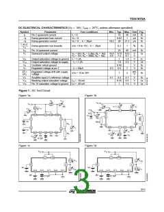
Pin 2
The supply of the power output stage is
forced at this pin. During the trace time
the supply voltage is obtained from the
main supply voltage VS by a diode,
while during the retrace time this pin is
supplied from the flyback generator.
Pin 7 The resistance between pin 7 and ground
defines the current mirror current and
than the height of the scanning.
Pin 9 is the output of the current mirror that
charges the series of Ca and Cb. This
pin is also the input of the buffer stage.
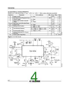
Flyback generator
This circuit supplies both the poweramplifier output
stage and the yoke during the most of the duration
of the flyback time (retrace).
Pin 10 is the output of the buffer stage and it is
internally coupled to the inverting input
of the power amplifier through R1.
The internal clock opens the loop of the amplifier
and lets pin 1 floating so allowing the rising of the
flyback. Crossingthe main supply voltageat pin14,
the flyback pulse front end drives the flyback
generator in such a way allowing its output to reach
and overcome the main supply voltage, starting
from a low condition forced during the trace period.
Power amplifier
This amplifier is a voltage-to-current power
converter, the transconductance of which is
externally defined by means of a negative current
feedback.
An integrated diode stops the rising of this output
increase and the voltage jump is transferred by
means of capacitor Cf at the supply voltage pin of
the power stage (pin 2).
The output stage of the power amplifier is supplied
by the main supply during the trace period, and by
the flyback generator circuit during the most of the
durationoftheflybacktime. The internal clock turns
off the lowerpower output stagetostarttheflyback.
When the current across the yoke changes its
direction, the output of the flyback generator falls
down to the main supply voltage and it is stopped
by means of the saturated output darlington at a
high level. At this time the flyback generator starts
to supply the power output amplifier output stage
by a diode inside the device. The flyback generator
supplies the yoke too.
The power output stage is thermally protected by
sensing the junction temperature and then by
putting off the current sources of the power stage.
Pin 12 is the inverting input of the amplifier.
An external network, Ra and Rb, defines
the DClevel across Cy so allowing a cor-
rect centering of the output voltage. The
series network Rc and Cc, in conjunction
with Ra and Rb, applies at the feedback
input I2 a small part of the parabola,
available across Cy, and AC feedback
voltage, taken across Rf. The external
components Rc, Ra and Rd, produce the
linearity correction on the output scan-
ning currentIy and their values must be
optimized for each type of CRT.
Later, the increasing flyback current reaches the
peak value and then the flyback time is completed:
the trace period restarts. The output of the power
amplifier (pin 1) falls under the main supply voltage
and the output of the flyback generator is driven for
a low state so allowing the flyback capacitor Cf to
restore the energy lost during the retrace.
Pin 15 is the output of the flyback generator that,
when driven, jumps from low to high
condition. An external capacitor Cf trans-
fers the jump to pin 2 (see pin 2).
Pin 11 is the non-inverting input. At this pin the
non-inverting input reference voltage
supplied by the voltage regulator can be
measured. A capacitor must be con-
nected to increase the performances
from the noise point of view.
Blanking generator and CRT protection
This circuit is a pulse shaper and its output goes
high during the blanking period or for CRT
protection.Theinputisinternallydrivenbytheclock
pulse that defines the width of the blanking time
Pin 1
is the output of the power amplifier and it
drives the yoke by a negative slope cur-
9/11

 STMICROELECTRONICS [ ST ]