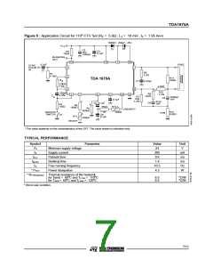
TDA1675A
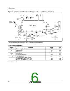
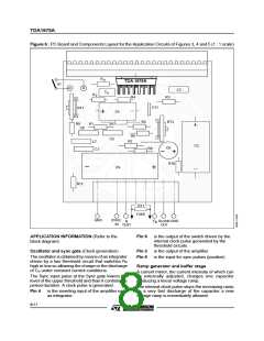
Figure 6 : PC Board and Components Layout for the Application Circuits of Figures 3, 4 and 5 (1 : 1 scale)
R
o
TDA 1675A
S1
C3
C
o
R
2
R4
R3
C11
RT1
C4
R5
RT2
R9
C6
R1
D1
C5
R6
R7
C7
C1
C2
C8
R8
R10
C9
R12
R11
YOKE
GND
SYNC.
IN
Iy
TEST
BLANK GND
OUT
V
S
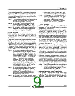
APPLICATION INFORMATION (Refer to the
block diagram)
Pin 6
is the output of the switch driven by the
internal clock pulse generated by the
threshold circuits.
Oscillator and sync gate (Clock generation)
Pin 3
Pin 5
is the output of the amplifier.
The oscillator is obtained by means of an integrator
driven by a two threshold circuit that switches Ro
high or low so allowing the charge or the discharge
of Co under constant current conditions.
is the input for sync pulses (positive)
Ramp generator and buffer stage
A current mirror, the current intensity of which can
be externally adjusted, charges one capacitor
producing a linear voltage ramp.
The Sync input pulse at the Sync gate lowers the
level of the upper threshold and than it controls the
period duration. A clock pulse is generated.
The internal clock pulse stops the increasing ramp
by a very fast discharge of the capacitor a new
voltage ramp is immediately allowed.
Pin 4 is the inverting input of the amplifier used
as integrator.
8/11

 STMICROELECTRONICS [ ST ]