TDA1675A
DC ELECTRICAL CHARACTERISTICS (VS = 35V, Tamb = 25oC, unless otherwise specified)
Symbol
I2
Parameter
Pin 2 quiescent current
Ramp generator bias current
Ramp generator current
Test conditions
Min. Typ. Max. Unit Fig.
I1 = 0
16
0.02
20
36
1
mA
µA
µA
1b
1b
1b
- I9
V9 = 0
- I9
V9 = 0 ; - I7 = 20µA
18.5
21.5
∆I 9
I 9
Ramp generator non linearity
∆V9 = 0 to 15V, - I7 = 20µA
0.2
1
%
1b
I14
Pin 14 quiescent current
Quiescent output voltage
25
45
mA
1b
1a
V1
VS = 35V, Ra = 2.2kΩ, Rb = 1kΩ
VS = 15V, Ra = 390Ω, Rb = 1kΩ
16.4 17.8 19.5
V
V
6.9
7.5
8.1
1.4
2.2
V1L
V1H
V4
Output saturation voltage to ground I1 = 1.2A,
1
V
V
V
V
1c
1d
1b
1b
Output saturation voltage to supply
Oscillator virtual ground
- I1 = 1.2A
1.6
0.45
6.6
V7
Regulated voltage at pin 7
- I7 = 20µA
6.3
4.1
7
2
∆V 7
∆VS
mV
V
Regulated voltage drift with supply
voltage
∆VS = 15 to 35V
1
1b
V11
V13
V15
Amplifier input (+) reference voltage
Blanking output saturation voltage
4.4
0.35
1
4.7
0.5
1.5
V
V
V
1b
1a
1a
I13 = 10 mA
Pin 15 saturation voltage to ground I15 = 20 mA
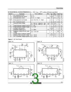
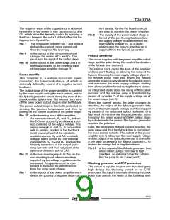
Figure 1 : DC Test Circuit.
Figure 1a
Figure 1b
I15
V15
VS
VS
V13
V11
I 2 + I 1
I 14
I13
A
B
11
14
2
7
4
4
I1
1
13
14
15
2
V4
1V
3
7
4
1
8V
1V
75kΩ
Ra
12
5
10
V7
9
8
V1
12
-I9
V9
9
5
11
8
10
Rb
-I7
-I9
0.1µF
Figure 1c
Figure 1d
VS
VS
14
14
2
2
+I 1
V1H
4
4
1
1
1V
1V
V1L
-I1
12
11
5
10
8
12
11
5
0.1µF
10
8
8V
8V
0.1µF
3/11

 STMICROELECTRONICS [ ST ]