T835H, T850H
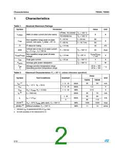
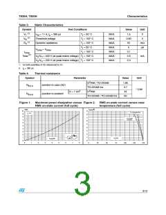
Characteristics
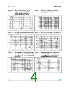
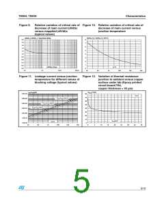
Figure 9.
Relative variation of critical rate of Figure 10. Relative variation of critical rate of
decrease of main current (dI/dt)c
versus reapplied (dV/dt)c
(typical values)
decrease of main current versus
junction temperature
(dI/dt)c [Tj] / (dI/dt)c [Tj=150°C]
(dI/dt)c [ (dV/dt)c ] / Specified (dI/dt)c
2.0
1.8
1.6
1.4
1.2
1.0
0.8
0.6
0.4
0.2
0.0
8
7
6
5
4
3
2
1
0
(dV/dt)C (V/µs)
Tj(°C)
0.1
1.0
10.0
100.0
25
50
75
100
125
150
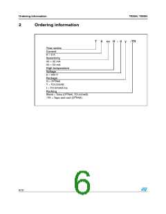
Figure 11. Leakage current versus junction
temperature for different values of
blocking voltage (typical values)
Figure 12. Variation of thermal resistance
junction to ambient versus copper
surface under tab (Epoxy printed
circuit board FR4,
copper thickness = 35 µm)
Rth(j-a)(°C/W)
IDRM/IRRM(µA)
1.0E+04
80
70
60
50
40
30
20
10
0
D²PAK
VDRM=VRRM=600 V
1.0E+03
1.0E+02
1.0E+01
1.0E+00
1.0E-01
1.0E-02
VDRM=VRRM=400 V
VDRM=VRRM=200 V
SCU(cm²)
Tj(°C)
25
50
75
100
125
150
0
5
10
15
20
25
30
35
40
5/10

 STMICROELECTRONICS [ ST ]