STM8S903K3 STM8S903F3
Electrical characteristics
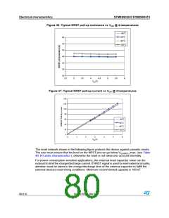
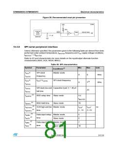
Figure 38: Recommended reset pin protection
STM8
VDD
RPU
External
reset
Internal reset
NRST
Filter
circuit
0.1 μF
(optional)
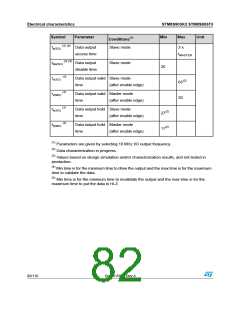
10.3.8
SPI serial peripheral interface
Unless otherwise specified, the parameters given in the following table are derived from tests
performed under ambient temperature, fMASTER frequency and VDD supply voltage conditions.
tMASTER = 1/fMASTER
.
Refer to I/O port characteristics for more details on the input/output alternate function
characteristics (NSS, SCK, MOSI, MISO).
Table 45: SPI characteristics
Symbol
Parameter
Min
Max
Unit
Conditions(1)
fSCK1/
tc(SCK)
SPI clock
frequency
Master mode
0
8
MHz
fSCK1/
tc(SCK)
fSCK1/ tc(SCK)
SPI clock frequency
0
7(2)
25
MHz
tr(SCK)
tf(SCK)
SPI clock rise and Capacitive load: C = 30 pF
fall time
(3)
tsu(NSS)
NSS setup time
Slave mode
4 x
tMASTER
(3)
th(NSS)
NSS hold time
Slave mode
70
(3)
tw(SCKH)
SCK high and low Master mode
time
tSCK
/
tSCK
/
ns
(3)
tw(SCKL)
2 - 15
2 +15
(3)
tsu(MI)
Data input setup Master mode
5
(3)
(3)
tsu(SI)
time
Slave mode
5
th(MI)
Data input hold
time
Master mode
Slave mode
7
(3)
th(SI)
10
DocID15590 Rev 8
81/116

 STMICROELECTRONICS [ ST ]