Electrical characteristics
STM8S903K3 STM8S903F3
Symbol Parameter
Data retention (data
Conditions
Typ
Max
Unit
Min(1)
memory) after 300k
erase/write cycles at
TA = +125 °C
TRET = 85°C
1
-
-
IDD
Supply current (Flash
programming or erasing
for 1 to 128 bytes)
-
2
-
mA
(1) Data based on characterization results, not tested in production.
(2) The physical granularity of the memory is 4 bytes, so cycling is performed on 4 bytes
even when a write/erase operation addresses a single byte.
10.3.6
I/O port pin characteristics
General characteristics
Subject to general operating conditions for VDD and TA unless otherwise specified. All unused
pins must be kept at a fixed voltage: using the output mode of the I/O for example or an
external pull-up or pull-down resistor.
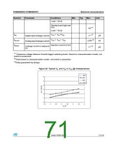
Table 40: I/O static characteristics
Symbol
Parameter
Conditions
Min
Typ
Max
0.3 x
VDD
Unit
VIL
VDD = 5 V
Input low level voltage
-0.3 V
-
V
VIH
VDD
0.3
+
0.7 x
VDD
Input high level voltage
-
Vhys
Rpu
Hysteresis(1)
-
700
-
mV
kΩ
VDD = 5 V, VIN = VSS
30
55
-
80
Pull-up resistor
tR, tF
Fast I/Os
35 (3)
Rise and fall time
(10 % - 90 %)
-
Load = 50 pF
Standard and high sink
I/Os
ns
125 (3)
20(3)
-
-
-
-
Load = 50 pF
Fast I/Os
70/116
DocID15590 Rev 8

 STMICROELECTRONICS [ ST ]