STM8S903K3 STM8S903F3
Symbol Parameter
Electrical characteristics
Max(1)
Conditions
Typ
Unit
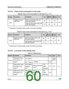
Wakeup time active MVR voltage
HSI
Flash in operating
mode(5)
48(6)
-
halt mode to run
mode(3)
regulator
off(4)
(after
wakeup)
Wakeup time active MVR voltage Flash in
HSI
50(6)
-
halt mode to run
mode(3)
regulator
off(4)
power-down
mode(5)
(after
wakeup)
Wakeup time from
halt mode to run
mode(3)
Flash in operating mode(5)
52
54
-
-
tWU(H)
Flash in power-down mode(5)
(1) Data guaranteed by design, not tested in production.
(2)
t
= 2 x 1/fmaster + 6 x 1/fCPU.
WU(WFI)
(3) Measured from interrupt event to interrupt vector fetch.
(4) Configured by the REGAH bit in the CLK_ICKR register.
(5) Configured by the AHALT bit in the FLASH_CR1 register.
(6) Plus 1 LSI clock depending on synchronization.
10.3.2.6 Total current consumption and timing in forced reset state
Table 32: Total current consumption and timing in forced reset state
Symbol
Parameter
Conditions
Typ
Unit
Max(1)
IDD(R)
Supply current in reset
state(2)
VDD = 5 V
400
300
-
-
μA
μs
VDD = 3.3 V
tRESETBL
Reset pin release to
vector fetch
-
150
(1) Data guaranteed by design, not tested in production.
(2) Characterized with all I/Os tied to VSS
.
10.3.2.7 Current consumption of on-chip peripherals
Subject to general operating conditions for VDD and TA.
DocID15590 Rev 8
61/116

 STMICROELECTRONICS [ ST ]