STM8S903K3 STM8S903F3
Product overview
program, specific code libraries, reset and interrupt vectors, the reset routine and usually the
IAP and communication routines.
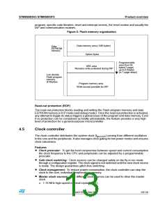
Figure 2: Flash memory organization
Data memory area ( 640 bytes)
Data
EEPROM
memory
Option bytes
Programmable
area from 64
UBC area
bytes(1 page)
Remains write protected during IAP
up to 8 Kbytes
(in 1 page steps)
Low density
Flash program
memory
(8 Kbytes)
Program memory area
Write access possible for IAP
Read-out protection (ROP)
The read-out protection blocks reading and writing the Flash program memory and data
EEPROM memory in ICP mode (and debug mode). Once the read-out protection is activated,
any attempt to toggle its status triggers a global erase of the program and data memory. Even
if no protection can be considered as totally unbreakable, the feature provides a very high
level of protection for a general purpose microcontroller.
4.5
Clock controller
The clock controller distributes the system clock (fMASTER) coming from different oscillators
to the core and the peripherals. It also manages clock gating for low power modes and ensures
clock robustness.
Features
Clock prescaler: To get the best compromise between speed and current consumption
the clock frequency to the CPU and peripherals can be adjusted by a programmable
prescaler.
•
Safe clock switching: Clock sources can be changed safely on the fly in run mode
through a configuration register. The clock signal is not switched until the new clock source
is ready. The design guarantees glitch-free switching.
•
Clock management: To reduce power consumption, the clock controller can stop the
clock to the core, individual peripherals or memory.
•
•
Master clock sources: Four different clock sources can be used to drive the master
clock:
1-16 MHz high-speed external crystal (HSE)
-
DocID15590 Rev 8
13/116

 STMICROELECTRONICS [ ST ]