Application block diagrams
STM32F405xx, STM32F407xx
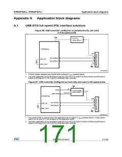
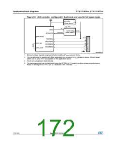
Figure 88. USB controller configured in dual mode and used in full speed mode
VDD
5 V to VDD
voltage regulator
(1)
VDD
EN
GPIO
5 V Pwr
Current limiter
(2)
Overcurrent
power switch
GPIO+IRQ
STM32F4xx
VBUS
PA9/PB13
DM
PA11/PB14
OSC_IN
DP
(3)
PA12/PB15
PA10/PB12
ID
OSC_OUT
V
SS
MS19002V3
1. External voltage regulator only needed when building a VBUS powered device.
2. The current limiter is required only if the application has to support a VBUS powered device. A basic power
switch can be used if 5 V are available on the application board.
3. The ID pin is required in dual role only.
4. The same application can be developed using the OTG HS in FS mode to achieve enhanced performance
thanks to the large Rx/Tx FIFO and to a dedicated DMA controller.
172/185
DocID022152 Rev 4

 STMICROELECTRONICS [ ST ]