STM32F405xx, STM32F407xx
Application block diagrams
Appendix A
Application block diagrams
A.1
USB OTG full speed (FS) interface solutions
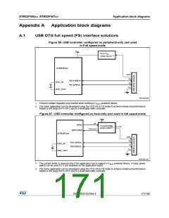
Figure 86. USB controller configured as peripheral-only and used
in Full speed mode
VDD
5V to VDD
Volatge regulator
(1)
STM32F4xx
VBUS
DM
DP
PA11//PB14
PA12/PB15
OSC_IN
V
SS
OSC_OUT
MS19000V5
1. External voltage regulator only needed when building a VBUS powered device.
2. The same application can be developed using the OTG HS in FS mode to achieve enhanced performance
thanks to the large Rx/Tx FIFO and to a dedicated DMA controller.
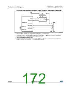
Figure 87. USB controller configured as host-only and used in full speed mode
VDD
EN
GPIO
Current limiter
5 V Pwr
(1)
power switch
Overcurrent
GPIO+IRQ
STM32F4xx
VBUS
DM
PA11//PB14
OSC_IN
DP
PA12/PB15
VSS
OSC_OUT
MS19001V4
1. The current limiter is required only if the application has to support a VBUS powered device. A basic power
switch can be used if 5 V are available on the application board.
2. The same application can be developed using the OTG HS in FS mode to achieve enhanced performance
thanks to the large Rx/Tx FIFO and to a dedicated DMA controller.
DocID022152 Rev 4
171/185

 STMICROELECTRONICS [ ST ]