STM32F302xx/STM32F303xx
Electrical characteristics
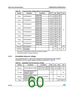
1. Data based on characterization results, not tested in production.
2. Guaranteed by design, not tested in production
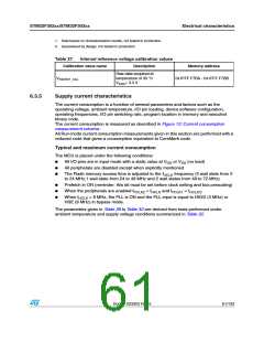
Table 27. Internal reference voltage calibration values
Calibration value name
Description
Memory address
Raw data acquired at
temperature of 30 °C
VREFINT_CAL
0x1FFF F7BA - 0x1FFF F7BB
VDDA= 3.3 V
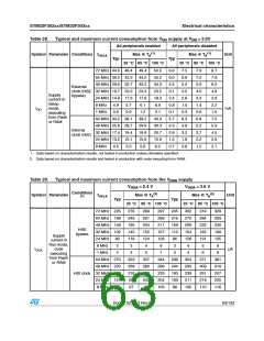
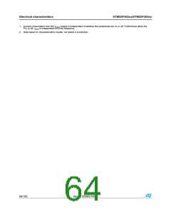
6.3.5
Supply current characteristics
The current consumption is a function of several parameters and factors such as the
operating voltage, ambient temperature, I/O pin loading, device software configuration,
operating frequencies, I/O pin switching rate, program location in memory and executed
binary code.
The current consumption is measured as described in Figure 12: Current consumption
measurement scheme.
All Run-mode current consumption measurements given in this section are performed with a
reduced code that gives a consumption equivalent to CoreMark code.
Typical and maximum current consumption
The MCU is placed under the following conditions:
●
●
●
All I/O pins are in input mode with a static value at V or V (no load)
DD SS
All peripherals are disabled except when explicitly mentioned
The Flash memory access time is adjusted to the f frequency (0 wait state from 0
HCLK
to 24 MHz,1 wait state from 24 to 48 MHz and 2 wait states from 48 to 72 MHz)
●
●
●
Prefetch in ON (reminder: this bit must be set before clock setting and bus prescaling)
When the peripherals are enabled f
= f
and f
= f
PCLK2
HCLK
PCLK1 HCLK/2
When f
> 8 MHz, the PLL is ON and the PLL input is equal to HSI/2 (4 MHz) or
HCLK
HSE (8 MHz) in bypass mode.
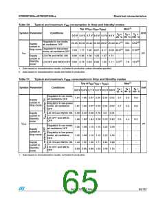
The parameters given in Table 28 to Table 32 are derived from tests performed under
ambient temperature and supply voltage conditions summarized in Table 22.
Doc ID 023353 Rev 5
61/133

 STMICROELECTRONICS [ ST ]