Electrical characteristics
STM32F302xx/STM32F303xx
6.3
Operating conditions
6.3.1
General operating conditions
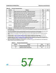
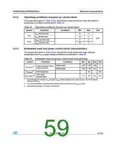
Table 22. General operating conditions
Symbol
Parameter
Conditions
Min
Max
Unit
fHCLK
fPCLK1
fPCLK2
VDD
Internal AHB clock frequency
Internal APB1 clock frequency
Internal APB2 clock frequency
Standard operating voltage
0
0
0
2
72
36
72
3.6
MHz
V
Analog operating voltage
(OPAMP and DAC not used)
2
3.6
Must have a potential
equal to or higher than
VDD
VDDA
V
V
Analog operating voltage
(OPAMP and DAC used)
2.4
3.6
3.6
VBAT
Backup operating voltage
1.65
TC I/O
–0.3 VDD+0.3
TTa I/O
–0.3
V
DDA+0.3
VIN
I/O input voltage
V
FT and FTf I/O(1)
–0.3
5.5
BOOT0
0
-
5.5
LQFP100
LQFP64
488
Power dissipation at TA =
85 °C for suffix 6 or TA =
105 °C for suffix 7(2)
PD
-
444
mW
°C
LQFP48
-
364
Maximum power
dissipation
–40
–40
–40
85
Ambient temperature for 6
suffix version
Low power dissipation(3)
105
105
TA
TJ
Maximum power
dissipation
Ambient temperature for 7
suffix version
°C
°C
Low power dissipation(3)
–40
–40
–40
125
105
125
6 suffix version
Junction temperature range
7 suffix version
1. To sustain a voltage higher than VDD+0.3 V, the internal pull-up/pull-down resistors must be disabled.
2. If TA is lower, higher PD values are allowed as long as TJ does not exceed TJmax (see Table 21: Thermal
characteristics).
3. In low power dissipation state, TA can be extended to this range as long as TJ does not exceed TJmax (see
Table 21: Thermal characteristics).
58/133
Doc ID 023353 Rev 5

 STMICROELECTRONICS [ ST ]