Pin description
STA8088EXG
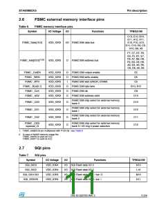
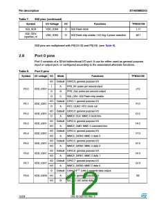
Table 7.
SQI pins (continued)
Symbol
I/O Voltage
I/O
Functions
TFBGA169
SQI_SCK
VDD_IOR4
O
SQI Flash clock
SQI Flash chip enable / I/O ring 4 power selection
L11
SQI_CEn/
iopwrsel_r4
VDD_IOR4
O
M11
SQI pins are multiplexed with P0[13:10] and P0[19] (see Table 8).
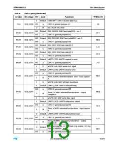
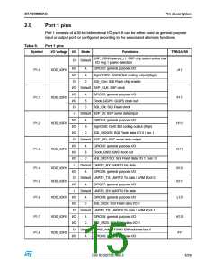
2.8
Port 0 pins
Port 0 consists of a 32-bit bidirectional I/O port. It can be either used as general purpose
input or output port, or configured according to the associated alternate functions.
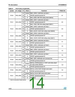
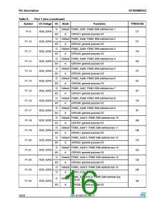
Table 8.
Port 0 pins
Symbol I/O voltage I/O
Mode
Functions
TFBGA169
I/O Default GPIO.0: general purpose I/O
I
A
B
C
PPS_IN: pulse per second input
PPS_Out: pulse per second output
SQI_CEn: SQI Flash chip enable
P0.0
VDD_IOR1
J13
O
O
I/O Default GPIO.1: general purpose I/O
RTC_CLKO: RTC clock out
I/O Default GPIO.2: general purpose I/O
MMC2_CLK: MMC 2 clock line
I/O Default GPIO.3: general purpose I/O
I/O MMC2_CMD: MMC 2 command line
I/O Default GPIO.4: general purpose I/O
I/O MMC2_DATA3: MMC 2 data 3
I/O Default GPIO.5: general purpose I/O
I/O MMC2_DATA2: MMC 2 data 2
I/O Default GPIO.6: general purpose I/O
I/O MMC2_DATA1: MMC 2 data 1
I/O Default GPIO.7: general purpose I/O
P0.1
P0.2
P0.3
P0.4
P0.5
P0.6
P0.7
VDD_IOR1
VDD_IOR1
VDD_IOR1
VDD_IOR1
VDD_IOR1
VDD_IOR1
VDD_IOR1
F12
E12
H12
F13
E13
H13
G13
O
A
O
A
A
A
A
A
I/O
O
A
MMC2_DATA0: MMC 2 data 0
Default CAN1TX(1): CAN 1 transmit data output
P0.8
VDD_IOR5 I/O
I/O
A
B
GPIO.8: general purpose I/O
I2C_SD: I2C serial data
B2
12/24
Doc ID 022725 Rev. 2

 STMICROELECTRONICS [ ST ]