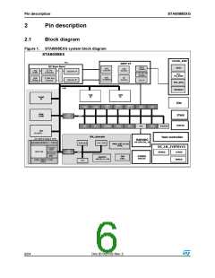
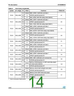
Pin description
STA8088EXG
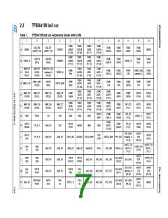
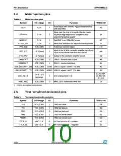
2.4
Main function pins
Table 4.
Main function pins
Symbol
I/O voltage
I/O
Functions
TFBGA169
Reset Input with Schmitt-Trigger characteristics
and noise filter.
RSTn
1.2 V
I
K8
When low, the chip is forced in Standby mode.
STDBYn
1.2 V
I
J6
All pins in high impedance except the ones
powered by backup supply
WAKEUP
STDBY_Out
PPS_Out
1.2 V
1.2 V
I
WAKEUP from STANDBY mode
K7
J5
O
O
When low, indicates the chip is in Standby mode.
Pulsed per second output
VDD_IOR1
J10
Input of the 32 KHz oscillator amplifier circuit and
input of the internal real time clock circuit.
RTC_XTI
1.5 V (max)
I
M9
RTC_XTO
CAN0TX(1)
CAN0RX(1)
1.5 V (max)
VDD_IOR5
VDD_IOR5
O
O
I
Output of the oscillator amplifier circuit.
CAN 0 - transmit data output
CAN 0 - receive data input
N9
A4
B4
A2
A3
USB_DM/UART1_RX VDD_IOR5
USB/I USB D- signal / UART 1 Rx data
USB/O USB D+ signal / UART 1 Tx data
USB_DP/UART1_TX
VDD_IOR5
L7, L9, M7,
L8, N8, M8,
N7, K9
1.4 V – 0 V
typ range
ADC_IN[1:8]
I
ADC analog input [1:8]
MMC_CLK
VDD_IOR2
O
MMC_CLK: multimedia clock line
D1
1. Only for Automotive Grade devices.
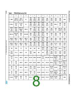
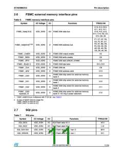
2.5
Test / emulated dedicated pins
Table 5.
Test/emulated dedicated pins
Symbol
I/O Voltage
I/O
Functions
TFBGA169
TCK
TDI
VDD_IOR5
VDD_IOR5
VDD_IOR5
VDD_IOR5
VDD_IOR5
VRF12_IF
VRF12_IF
I
I
JTAG test clock
G4
G3
H4
G1
G2
H2
J2
JTAG test data in
JTAG test data out
TDO
O
I
TMS
JTAG test mode select
TRSTn
TP_IF_P
TP_IF_N
I
JTAG test circuit reset
O
O
Diff. test point for IF – positive
Diff. test point for IF – negative
10/24
Doc ID 022725 Rev. 2

 STMICROELECTRONICS [ ST ]