STA335BW
Connection diagram and pin description
2
Connection diagram and pin description
2.1
Connection diagram
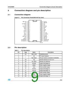
Figure 2.
Pin connection PowerSSO-36 (Top view)
1
2
36
35
34
33
32
31
30
29
28
27
26
25
24
23
22
21
20
19
GND_SUB
SA
V
dd_DIG
GND_DIG
TEST MODE
VSS
3
SCL
4
SDA
5
INT_LINE
RESET
VCC_REG
OUT2B
GND2
6
7
SDI
8
VCC2
LRCKI
9
OUT2A
OUT1B
BICKI
10
11
12
13
14
15
16
17
18
XTI
PLL_GND
PLL_FILTER
PLL_Vdd
POWRDN
GND_DIG
VDD_DIG
TWARN/OUT4B
EAPD/OUT4A
V
CC1
GND1
OUT1A
GND_REG
Vdd
CONFIG
OUT3B/DDX3B
OUT3A/DDX3A
D05AU1605
2.2
Pin description
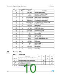
Table 1.
Pin
Pin description
Type
Name
Description
1
2
I/O
I
GND_SUB
SA
Substrate ground
I2C Select Address
3
I
Test_Mode
Vss
This pin must be connected to GROUND
Internal reference at Vcc-3.3 V
Internal Vcc reference
Output half bridge 2B
4
I/O
I/O
O
5
Vcc_REG
OUT2B
GND2
6
7
I/O
I/O
O
Power negative supply
Power positive supply
8
Vcc2
9
OUT2A
OUT1B
Vcc1
Output half bridge 2A
10
11
12
13
O
Output half bridge 1B
I/O
I/O
I/O
Power positive supply
GND1
Power negative supply
Output half bridge 1A
OUT1A
9/54

 STMICROELECTRONICS [ ST ]