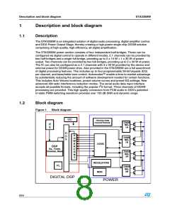
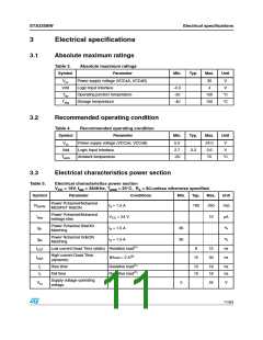
Electrical specifications
STA335BW
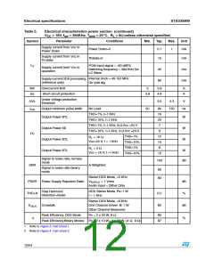
Table 5.
Symbol
Electrical characteristics power section (continued)
V
= 18V, f = 384KHz, T
= 25°C, R = 8Ω unless otherwise specified.
CC
sw
amb L
Parameter
Conditions
Min.
Typ.
Max.
Unit
Supply current from Vcc in
Power Down
Power Down=0
Tristate=0
0.1
1
mA
Supply current from Vcc in
Tri-state
15
40
80
mA
mA
mA
Icc
PCM Input signal = -60 dBFS.
Switching frequency = 384 KHz No
LC filters
Supply current from Vcc in
operation
Internal clock = 49.152 MHz
On Vdd dig
Supply current DDX processing
(reference only)
Ilim
Isc
Overcurrent limit
3
3.8
4.8
A
A
Short circuit protection
3.8
Under voltage protection
threshold
UVL
tmin
3.5
4.3
V
Output minimum pulse width
No Load
50
80
16
20
7
150
ns
THD=1%, f=1 KHz
Output Power BTL
W
W
W
THD=10%, f=1 KHz
THD=1%, f=1 KHz, 8 Ω Vcc =24 V
THD=10%, f=1 KHz, 8 Ω Vcc =24 V
Output Power SE
Output Power BTL
Output Power BTL
9
Po
THD=1%
12
15
8
RL = 16 Ω
Vcc=24 V; f = 1 KHz
THD=10%
THD=1%
THD=10%
RL = 4 Ω
Vcc = 18 V; f =1 KHz
W
10
Signal to noise ratio, ternary
mode
100
dB
SNR
A-Weighted
Signal to noise ratio binary
mode
90
80
Stereo DDX Mode, <5 KHz
PSSR Power Supply Rejection Ratio VRIPPLE = 1 Vrms
Audio Input = Dither Only
dB
%
DDX Stereo Mode, Po=1 W
f = 1 KHz
Total Harmonic
Distortion+Noise
THD+N
XTALK
0.2
80
Stereo DDX Mode, <5 KHz
One Channel Driven @ 1 W
Other Channel Measured
Crosstalk
dB
Peak Efficiency, DDX Mode
Po = 2 x 20 W, 8 Ω
90
87
η
%
Peak Efficiency,Binary Modes Po = 2 x 10 W+ 1 x 20 W, (4 Ω, 8 Ω)
1. Refer to Figure 3: Test circuit 1.
2. Refer to Figure 4: Test circuit 2.
12/54

 STMICROELECTRONICS [ ST ]