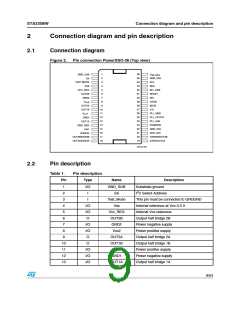
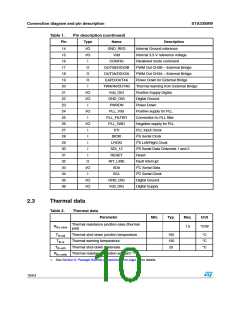
Connection diagram and pin description
STA335BW
Table 1.
Pin
Pin description (continued)
Type
Name
Description
Internal Ground reference
14
15
16
17
18
19
20
21
22
23
24
25
26
27
28
29
30
31
32
33
34
35
36
I/O
I/O
I
GND_REG
Vdd
Internal 3.3 V reference voltage
Paralleled mode command
CONFIG
OUT3B/DDX3B
OUT3A/DDX3A
EAPD/OUT4A
TWARN/OUT4B
Vdd_DIG
GND_DIG
PWRDN
O
O
O
I
PWM Out CH3B – External Bridge
PWM Out CH3A – External Bridge
Power Down for External Bridge
Thermal warning from External Bridge
Positive Supply Digital
Digital Ground
I/O
I/O
I
Power Down
I/O
I
PLL_Vdd
PLL_FILTER
PLL_GND
XTI
Positive supply for PLL
Connection to PLL filter
Negative supply for PLL
PLL Input Clock
I/O
I
I
BICKI
I2S Serial Clock
I
LRCKI
I2S Left/Right Clock
I2S Serial Data Channels 1 and 2
Reset
I
SDI_12
I
RESET
O
I/O
I
INT_LINE
SDA
Fault Interrupt
I2C Serial Data
SCL
I2C Serial Clock
I/O
I/O
GND_DIG
Vdd_DIG
Digital Ground
Digital Supply
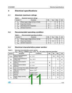
2.3
Thermal data
Table 2.
Thermal data
Parameter
Min.
Typ.
Max.
Unit
Thermal resistance junction-case (thermal
pad)
Rth j-case
1.5
°C/W
Tth-sdj
Tth-w
Thermal shut-down junction temperature
Thermal warning temperature
150
130
25
°C
°C
°C
Tth-sdh
Thermal shut-down hysteresis
Rth j-amb Thermal resistance junction-ambient (1)
1. See Section 6: Package thermal characteristics on page 51 for details.
10/54

 STMICROELECTRONICS [ ST ]