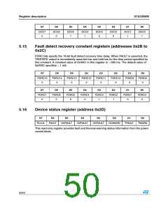
STA335BW
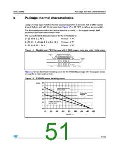
Package thermal characteristics
6
Package thermal characteristics
Using a double layer PCB the thermal resistance junction to ambient with 2 GND copper
area of 3x3 cm and with 16 via holes (see Figure 12) is 24 °C/W in natural air convection.
The dissipated power within the device depends primarily on the supply voltage, load
impedance and output modulation level.
The max estimated dissipated power for the STA335BW is:
2 x 20 W @ 8 Ω, 18 V
Pd max ~ 4 W
Pd max < 5 W
Pd max ~ 3 W
2 x 10 W + 1 x 20 W @ 4 Ω, 8 Ω, 18 V
2 x 15 W @ 16 Ω, 24 V
Figure 12. Double layer PCB R
with 2 GND copper area and with 16 via holes
th j-amb
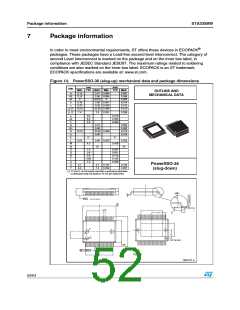
Figure 13 shows the Power Derating curve for the PSSO36 package with two copper areas
on board 2 x 2 cm and 3 x 3 cm.
Figure 13. PSSO36 power derating curve
8
7
6
5
4
3
2
1
0
Pd (W)
Copper Area 3x3 cm
and via holes
STA335BW
PSSO36
Copper Area 2x2 cm
and via holes
0
20 40 60 80 100 120 140 160
Tamb ( °C)
51/54

 STMICROELECTRONICS [ ST ]