STA335BW
Register description
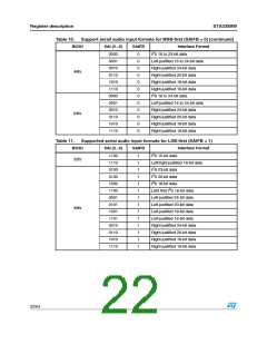
Table 11. Supported serial audio input formats for LSB-first (SAIFB = 1) (continued)
BICKI
SAI (3...0)
SAIFB
Interface Format
0000
0100
1000
1100
0001
0101
1001
1101
0010
0110
1010
1110
1
1
1
1
1
1
1
1
1
1
1
1
I2S 24-bit data
I2S 20-bit data
I2S 18-bit data
LSB first I2S 16-bit data
Left-justified 24-bit data
Left-justified 20-bit data
Left-justified 18-bit data
Left-justified 16-bit data
Right-justified 24-bit data
Right-justified 20-bit data
Right-justified 18-bit data
Right-justified 16-bit data
64fs
5.2.4
5.2.5
Delay serial clock enable
Bit
R/W
RST
Name
Description
0 – No serial clock delay
5
R/W
0
DSCKE
1 – Serial clock delay by 1 core clock cycle to
tolerate anomalies in some I2S master devices
Channel input mapping
Bit
R/W
RST
Name
Description
0 – Processing channel 1 receives Left I2S Input
1 – Processing channel 1 receives Right I2S Input
6
R/W
0
C1IM
0 – Processing channel 2 receives Left I2S Input
1 – Processing channel 2 receives Right I2S Input
7
R/W
1
C2IM
2
Each channel received via I S can be mapped to any internal processing channel via the
Channel Input Mapping registers. This allows for flexibility in processing. The default
2
settings of these registers map each I S input channel to its corresponding processing
channel.
23/54

 STMICROELECTRONICS [ ST ]