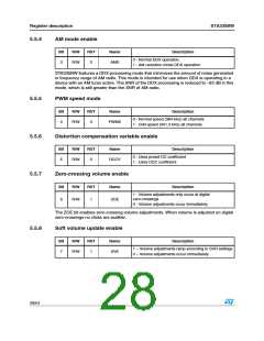
Register description
STA335BW
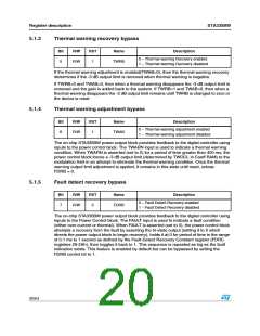
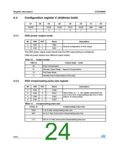
5.3
Configuration register C (Address 0x02)
D7
D6
D5
D4
D3
D2
D1
D0
OCRB
1
CSZ3
0
CSZ2
1
CSZ1
0
CSZ0
1
OM1
1
OM0
1
5.3.1
DDX power output mode
Bit
R/W
RST
Name
Description
0
1
R/W
R/W
1
1
OM0
OM1
Selects configuration of DDX output.
The DDX power output mode selects how the DDX output timing is configured.
Different power devices use different output modes.
Table 12. Output modes
OM(1,0)
Output stage – mode
00
01
10
11
Drop Compensation
Discrete Output Stage – Tapered Compensation
Full Power Mode
Variable Drop Compensation (CSZx bits)
5.3.2
DDX compensating pulse size register
Bit
R/W
RST
Name
Description
2
3
4
5
R/W
R/W
R/W
R/W
1
0
1
0
CSZ0
CSZ1
CSZ2
CSZ3
When OM(1,0) = 11, this register determines the
size of the DDX compensating pulse from 0 clock
ticks to 15 clock periods.
Table 6:
Table 13. Compensating pulse size
CSZ(3..0)
Compensating Pulse Size
0000
0001
…
0 ns (0 tick) compensating pulse size
20 ns (1 tick) clock period compensating pulse size
…
1111
300 ns (15 tick) clock period compensating pulse size
24/54

 STMICROELECTRONICS [ ST ]