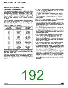
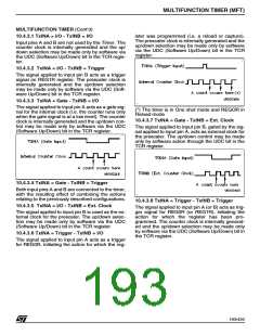
MULTIFUNCTION TIMER (MFT)
MULTIFUNCTION TIMER (Cont’d)
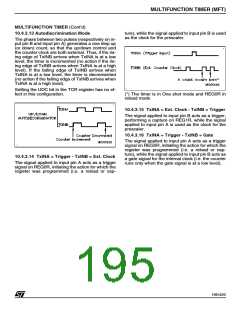
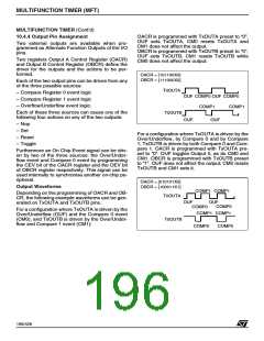
10.4.4 Output Pin Assignment
OACR is programmed with TxOUTA preset to “0”,
OUF sets TxOUTA, CM0 resets TxOUTA and
CM1 does not affect the output.
OBCR is programmed with TxOUTB preset to “0”,
OUF sets TxOUTB, CM1 resets TxOUTB while
CM0 does not affect the output.
Two external outputs are available when pro-
grammed as Alternate Function Outputs of the I/O
pins.
Two registers Output A Control Register (OACR)
and Output B Control Register (OBCR) define the
driver for the outputs and the actions to be per-
formed.
OACR = [101100X0]
OBCR = [111000X0]
Each of the two output pins can be driven from any
of the three possible sources:
T0OUTA
– Compare Register 0 event logic
– Compare Register 1 event logic
– Overflow/Underflow event logic.
OUF COMP0 OUF COMP0
COMP1
COMP1
Each of these three sources can cause one of the
following four actions on any of the two outputs:
T0OUTB
OUF
OUF
– Nop
– Set
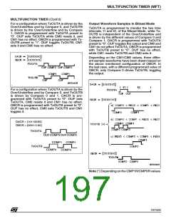
For a configuration where TxOUTA is driven by the
Over/Underflow, by Compare 0 and by Compare
1; TxOUTB is driven by both Compare 0 and Com-
pare 1. OACR is programmed with TxOUTA pre-
set to “0”. OUF toggles Output 0, as do CM0 and
CM1. OBCR is programmed with TxOUTB preset
to “1”. OUF does not affect the output; CM0 resets
TxOUTB and CM1 sets it.
– Reset
– Toggle
Furthermore an On Chip Event signal can be driv-
en by two of the three sources: the Over/Under-
flow event and Compare 0 event by programming
the CEV bit of the OACR register and the OEV bit
of OBCR register respectively. This signal can be
used internally to synchronise another on-chip pe-
ripheral.
OACR = [010101X0]
Output Waveforms
OBCR = [100011X1]
COMP1 COMP1
Depending on the programming of OACR and OB-
CR, the following example waveforms can be gen-
erated on TxOUTA and TxOUTB pins.
T0OUTA
OUF
COMP0
OUF
COMP0
For a configuration where TxOUTA is driven by the
Over/Underflow (OUF) and the Compare 0 event
(CM0), and TxOUTB is driven by the Over/Under-
flow and Compare 1 event (CM1):
COMP1 COMP1
T0OUTB
COMP0
COMP0
196/426
9

 STMICROELECTRONICS [ ST ]