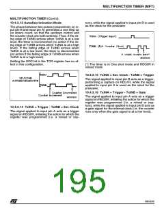
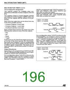
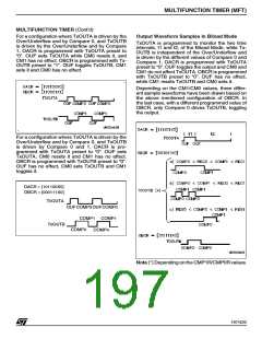
MULTIFUNCTION TIMER (MFT)
MULTIFUNCTION TIMER (Cont’d)
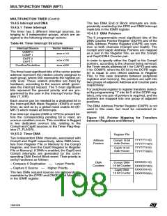
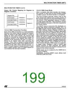
Figure 105. Pointer Mapping for Register to
Register Transfers
10.4.5.5 DMA Swap Mode
After a complete data table transfer, the transac-
tion counter is reset and an End Of Block (EOB)
condition occurs, the block transfer is completed.
Register File
The End Of Block Interrupt routine must at this
point reload both address and counter pointers of
the channel referred to by the End Of Block inter-
rupt source, if the application requires a continu-
ous high speed data flow. This procedure causes
speed limitations because of the time required for
the reload routine.
8 bit Counter
XXXXXX11
XXXXXX10
XXXXXX01
XXXXXX00
Compare 0
Capture 0
8 bit Addr Pointer
8 bit Counter
8 bit Addr Pointer
The SWAP feature overcomes this drawback, al-
lowing high speed continuous transfers. Bit 2 of
the DMA Counter Pointer Register (DCPR) and of
the DMA Address Pointer Register (DAPR), tog-
gles after every End Of Block condition, alternately
providing odd and even address (D2-D7) for the
pair of pointers, thus pointing to an updated pair,
after a block has been completely transferred. This
allows the User to update or read the first block
and to update the pointer values while the second
is being transferred. These two toggle bits are soft-
ware writable and readable, mapped in DCPR bit 2
for the CM0 channel, and in DAPR bit 2 for the
CP0 channel (though a DMA event on a channel,
in Swap mode, modifies a field in DAPR and
DCPR common to both channels, the DAPR/
DCPR content used in the transfer is always the bit
related to the correct channel).
10.4.5.4 DMA Transaction Priorities
Each Timer DMA transaction is a 16-bit operation,
therefore two bytes must be transferred sequen-
tially, by means of two DMA transfers. In order to
speed up each word transfer, the second byte
transfer is executed by automatically forcing the
peripheral priority to the highest level (000), re-
gardless of the previously set level. It is then re-
stored to its original value after executing the
transfer. Thus, once a request is being serviced,
its hardware priority is kept at the highest level re-
gardless of the other Timer internal sources, i.e.
once a Comp0 request is being serviced, it main-
tains a higher priority, even if a Capt0 request oc-
curs between the two byte transfers.
SWAP mode can be enabled by the SWEN bit in
the IDCR Register.
WARNING: Enabling SWAP mode affects both
channels (CM0 and CP0).
199/426
9

 STMICROELECTRONICS [ ST ]