MULTIFUNCTION TIMER (MFT)
MULTIFUNCTION TIMER (Cont’d)
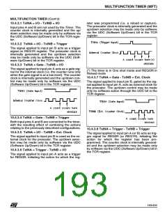
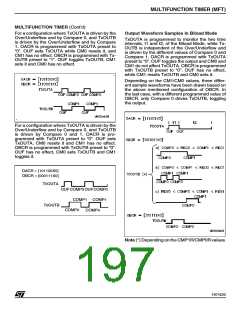
10.4.3.1 TxINA = I/O - TxINB = I/O
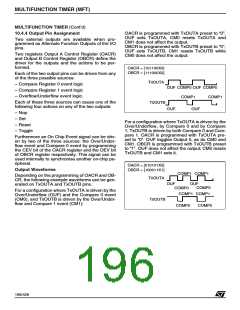
ister was programmed (i.e. a reload or capture).
The prescaler clock is internally generated and the
up/down selection may be made only by software
via the UDC (Software Up/Down) bit in the TCR
register.
Input pins A and B are not used by the Timer. The
counter clock is internally generated and the up/
down selection may be made only by software via
the UDC (Software Up/Down) bit in the TCR regis-
ter.
10.4.3.2 TxINA = I/O - TxINB = Trigger
The signal applied to input pin B acts as a trigger
signal on REG1R register. The prescaler clock is
internally generated and the up/down selection
may be made only by software via the UDC (Soft-
ware Up/Down) bit in the TCR register.
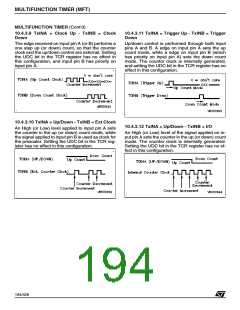
10.4.3.3 TxINA = Gate - TxINB = I/O
The signal applied to input pin A acts as a gate sig-
nal for the internal clock (i.e. the counter runs only
when the gate signal is at a low level). The counter
clock is internally generated and the up/down con-
trol may be made only by software via the UDC
(Software Up/Down) bit in the TCR register.
(*) The timer is in One shot mode and REGOR in
Reload mode
10.4.3.7 TxINA = Gate - TxINB = Ext. Clock
The signal applied to input pin B, gated by the sig-
nal applied to input pin A, acts as external clock for
the prescaler. The up/down control may be made
only by software action through the UDC bit in the
TCR register.
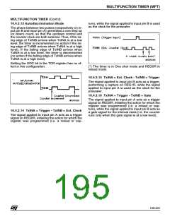
10.4.3.4 TxINA = Gate - TxINB = Trigger
Both input pins A and B are connected to the timer,
with the resulting effect of combining the actions
relating to the previously described configurations.
10.4.3.8 TxINA = Trigger - TxINB = Trigger
10.4.3.5 TxINA = I/O - TxINB = Ext. Clock
The signal applied to input pin A (or B) acts as trig-
ger signal for REG0R (or REG1R), initiating the
action for which the register has been pro-
grammed. The counter clock is internally generat-
ed and the up/down selection may be made only
by software via the UDC (Software Up/Down) bit in
the TCR register.
The signal applied to input pin B is used as the ex-
ternal clock for the prescaler. The up/down selec-
tion may be made only by software via the UDC
(Software Up/Down) bit in the TCR register.
10.4.3.6 TxINA = Trigger - TxINB = I/O
The signal applied to input pin A acts as a trigger
for REG0R, initiating the action for which the reg-
193/426
9

 STMICROELECTRONICS [ ST ]