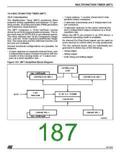
MULTIFUNCTION TIMER (MFT)
MULTIFUNCTION TIMER (Cont’d)
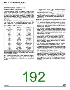
The configuration of each input is programmed in
the Input Control Register.
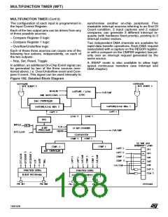
synchronise another on-chip peripheral. Five
maskable interrupt sources referring to an End Of
Count condition, 2 input captures and 2 output
compares, can generate 3 different interrupt re-
quests (with hardware fixed priority), pointing to 3
interrupt routine vectors.
Each of the two output pins can be driven from any
of three possible sources:
– Compare Register 0 logic
– Compare Register 1 logic
– Overflow/Underflow logic
Two independent DMA channels are available for
rapid data transfer operations. Each DMA request
(associated with a capture on the REG0R register,
or with a compare on the CMP0R register) has pri-
ority over an interrupt request generated by the
same source.
Each of these three sources can cause one of the
following four actions, independently, on each of
the two outputs:
– Nop, Set, Reset, Toggle
A SWAP mode is also available to allow high
speed continuous transfers (see Interrupt and
DMA chapter).
In addition, an additional On-Chip Event signal can
be generated by two of the three sources men-
tioned above, i.e. Over/Underflow event and Com-
pare 0 event. This signal can be used internally to
Figure 102. Detailed Block Diagram
188/426
9

 STMICROELECTRONICS [ ST ]