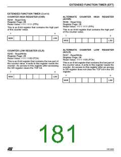
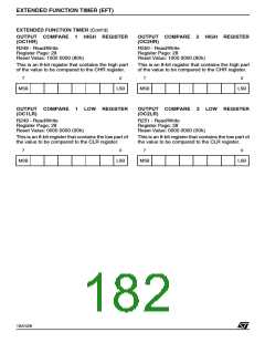
EXTENDED FUNCTION TIMER (EFT)
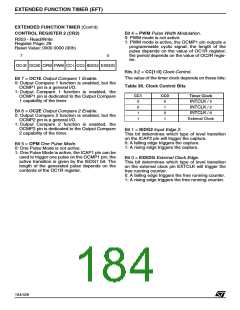
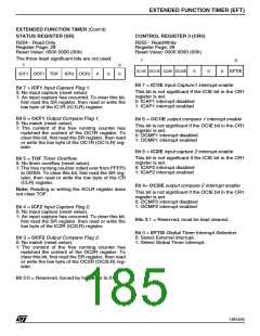
CONTROL REGISTER 3 (CR3)
EXTENDED FUNCTION TIMER (Cont’d)
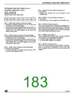
STATUS REGISTER (SR)
R254 - Read Only
R255 - Read/Write
Register Page: 28
Register Page: 28
Reset Value: 0000 0000 (00h)
Reset Value: 0000 0000 (00h)
The three least significant bits are not used.
7
7
0
0
0
IC1IE OC1IE IC2IE OC2IE
0
0
0
EFTIS
ICF1 OCF1 TOF ICF2 OCF2
0
0
Bit 7 = IC1IE Input Capture1 interrupt enable
Bit 7 = ICF1 Input Capture Flag 1.
This bit is not significant if the ICIE bit in the CR1
register is set.
0: ICAP1 interrupt disabled
1: ICAP1 interrupt enabled
0: No input capture (reset value).
1: An input capture has occurred. To clear this bit,
first read the SR register, then read or write the
low byte of the IC1R (IC1LR) register.
Bit 6 = OCF1 Output Compare Flag 1.
0: No match (reset value).
1: The content of the free running counter has
matched the content of the OC1R register. To
clear this bit, first read the SR register, then read
or write the low byte of the OC1R (OC1LR) reg-
ister.
Bit 6 = OC1IE output compare 1 interrupt enable
This bit is not significant if the OCIE bit in the CR1
register is set.
0: OCMP1 interrupt disabled
1: OCMP1 interrupt enabled
Bit 5 = IC2IE input capture 2 interrupt enable
This bit is not significant if the ICIE bit in the CR1
register is set.
0: ICAP2 interrupt disabled
1: ICAP2 interrupt enabled
Bit 5 = TOF Timer Overflow.
0: No timer overflow (reset value).
1:The free running counter rolled over from FFFFh
to 0000h. To clear this bit, first read the SR reg-
ister, then read or write the low byte of the CR
(CLR) register.
Bit 4= OC2IE output compare 2 interrupt enable
Note: Reading or writing the ACLR register does
not clear TOF.
This bit is not significant if the OCIE bit in the CR1
register is set.
0: OCMP2 interrupt disabled
1: OCMP2 interrupt enabled
Bit 4 = ICF2 Input Capture Flag 2.
0: No input capture (reset value).
1: An input capture has occurred. To clear this bit,
first read the SR register, then read or write the
low byte of the IC2R (IC2LR) register.
Bits 3:1 = Reserved, must be kept cleared.
Bit 0 = EFTIS Global Timer Interrupt Selection.
0: Select External interrupt.
1: Select Global Timer Interrupt.
Bit 3 = OCF2 Output Compare Flag 2.
0: No match (reset value).
1: The content of the free running counter has
matched the content of the OC2R register. To
clear this bit, first read the SR register, then read
or write the low byte of the OC2R (OC2LR) reg-
ister.
Bit 2:0 = Reserved, forced by hardware to 0.
185/426
9

 STMICROELECTRONICS [ ST ]