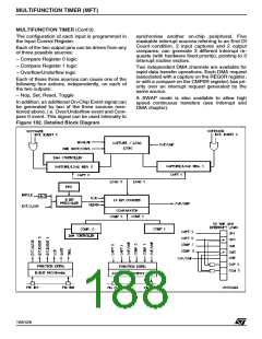
EXTENDED FUNCTION TIMER (EFT)
EXTENDED FUNCTION TIMER (Cont’d)
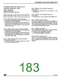
CONTROL REGISTER 2 (CR2)
Bit 4 = PWM Pulse Width Modulation.
0: PWM mode is not active.
1: PWM mode is active, the OCMP1 pin outputs a
programmable cyclic signal; the length of the
pulse depends on the value of OC1R register;
the period depends on the value of OC2R regis-
ter.
R253 - Read/Write
Register Page: 28
Reset Value: 0000 0000 (00h)
7
0
OC1E OC2E OPM PWM CC1 CC0 IEDG2 EXEDG
Bits 3:2 = CC[1:0] Clock Control.
The value of the timer clock depends on these bits:
Bit 7 = OC1E Output Compare 1 Enable.
0: Output Compare 1 function is enabled, but the
OCMP1 pin is a general I/O.
Table 36. Clock Control Bits
1: Output Compare 1 function is enabled, the
OCMP1 pin is dedicated to the Output Compare
1 capability of the timer.
CC1
CC0
Timer Clock
INTCLK / 4
INTCLK / 2
INTCLK / 8
External Clock
0
0
1
1
0
1
0
1
Bit 6 = OC2E Output Compare 2 Enable.
0: Output Compare 2 function is enabled, but the
OCMP2 pin is a general I/O.
1: Output Compare 2 function is enabled, the
OCMP2 pin is dedicated to the Output Compare
2 capability of the timer.
Bit 1 = IEDG2 Input Edge 2.
This bit determines which type of level transition
on the ICAP2 pin will trigger the capture.
0: A falling edge triggers the capture.
Bit 5 = OPM One Pulse Mode.
0: One Pulse Mode is not active.
1: A rising edge triggers the capture.
1: One Pulse Mode is active, the ICAP1 pin can be
used to trigger one pulse on the OCMP1 pin; the
active transition is given by the IEDG1 bit. The
length of the generated pulse depends on the
contents of the OC1R register.
Bit 0 = EXEDG External Clock Edge.
This bit determines which type of level transition
on the external clock pin EXTCLK will trigger the
free running counter.
0: A falling edge triggers the free running counter.
1: A rising edge triggers the free running counter.
184/426
9

 STMICROELECTRONICS [ ST ]