ST92F124/F150/F250 - RESET AND CLOCK CONTROL UNIT (RCCU)
CERAMIC RESONATORS
Murata Electronics CERALOCK resonators have been tested with the ST92F150 at 3, 3.68, 4 and 5 MHz.
These recommended resonators have built-in capacitors (see Table 32).
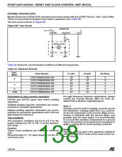
The test circuit is shown in Figure 69.
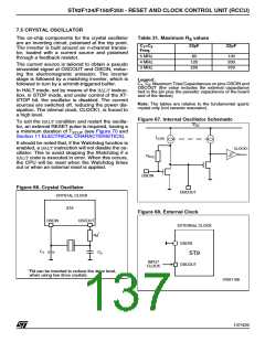
Figure 69. Test Circuit
ST92F150
V
DD
V
OSCIN
OSCOUT
SS
Rd
CERALOCK
C1 C2
Table 32 shows the recommended conditions at different frequencies.
Table 32. Obtained Results
Freq.
Parts Number
C1 (pF)
C2 (pF)
Rd (Ohm)
(MHz)
CSTCR5M00G55A-R0
CSTCC5M00G56A-R0
CSTCR4M00G55A-R0
CSTCC4M00G56A-R0
CSTCC3M00G56A-R0
CSTCC3M68G56A-R0
39
47
39
47
47
47
39
47
39
47
47
47
0
0
0
0
0
0
5
4
3
3.68
Advantages of using ceramic resonators:
For tight frequency tolerance applications, please
contact the nearest Murata office for more de-
tailled PCB evaluation regarding layout.
CSTCR and CSTCC types have built-in loading
capacitors.
Smallest loading capacitor resonators are recom-
mended for standard applications.
Note 1:
Attention must be paid to leakage currents around
Highest loading capacitor resonators are recom-
mended for automotive applications with CAN and
tight frequency tolerance.
the OSCIN pin. Leakage paths from V could al-
DD
ter the DC polarization of the inverter stage and in-
troduce a mismatch with the second stage, and
possibly stop the clock signal. It is recommended
to surround the oscillator components by a ground
ring on the printed circuit board and if necessary to
apply a coating film to avoid humidity problems.
Test conditions:
The evaluation conditions are 4.5 to 5.5 V for the
supply voltage and -40° to 105° C for the tempera-
ture range.
Caution:
Note 2:
These circuit conditions are for design reference
Attention must be paid to the capacitive loading of
OSCOUT. OSCOUT must not be used to drive ex-
ternal circuits.
only.
Recommended C1, C2 value depends on the cir-
cuit board used.
138/426
9

 STMICROELECTRONICS [ ST ]