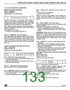
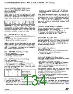
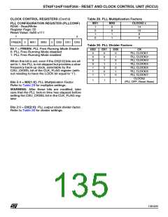
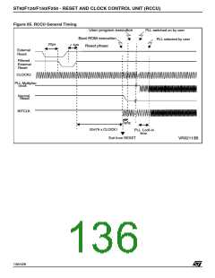
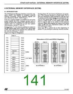
ST92F124/F150/F250 - RESET AND CLOCK CONTROL UNIT (RCCU)
7.5 CRYSTAL OSCILLATOR
The on-chip components for the crystal oscillator
are an inverting circuit, polarised at the trip point.
The inverter is built around an n-channel transis-
tor, loaded with a current source and polarised
through a feedback resistor.
Table 31. Maximum R values
S
C =C
33pF
22pF
1
2
Freq.
5 MHz
4 MHz
3 MHz
80
130
200
370
120
220
The current source is tailored to obtain a pseudo
sinusoidal signal at OSCOUT and OSCIN, reduc-
ing the electromagnetic emission. The inverter
stage is followed by a matching inverter, which is
followed in turn by a schmitt-triggered buffer.
Legend:
C , C : Maximum Total Capacitances on pins OSCIN and
1
2
OSCOUT (the value includes the external capacitance
tied to the pin plus the parasitic capacitance of the board
and of the device)
In HALT mode, set by means of the HALTinstruc-
tion, in STOP mode, and under control of the XT-
STOP bit, the oscillator is disabled. The current
sources are switched off, reducing the power dis-
sipation. The internal clock, CLOCK1, is forced to
a high level.
Note: The tables are relative to the fundamental quartz
crystal only (not ceramic resonator).
Figure 67. Internal Oscillator Schematic
To exit the HALTcondition and restart the oscilla-
tor, an external RESET pulse is required, having a
V
DD
a minimum duration of T
(see Figure 70 and
STUP
Section 11 ELECTRICAL CHARACTERISTICS).
I
LOAD
It should be noted that, if the Watchdog function is
enabled, a HALTinstruction will not disable the os-
cillator. This to avoid stopping the Watchdog if a
HALTcode is executed in error. When this occurs,
the CPU will be reset when the Watchdog times
out or when an external reset is applied.
CLOCK1
R
POL
OSCIN
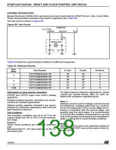
Figure 66. Crystal Oscillator
OSCOUT
CRYSTAL CLOCK
ST9
Figure 68. External Clock
OSCOUT
OSCIN
EXTERNAL CLOCK
*
Rd
OSCIN
C
C
1
2
ST9
INPUT
CLOCK
OSCOUT
*Rd can be inserted to reduce the drive level,
when using low drive crystals.
VR02116B
137/426
9

 STMICROELECTRONICS [ ST ]