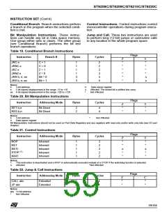
ST6208C/ST6209C/ST6210C/ST6220C
A/D CONVERTER (Cont’d)
8.3.5 Low Power Modes
cally cleared when the STA bit is set. Data in the
data conversion register are valid only when this
bit is set to “1”.
Mode
Description
0: Conversion is not complete
1: Conversion can be read from the ADR register
No effect on A/D Converter. ADC interrupts
cause the device to exit from Wait mode.
WAIT
STOP
A/D Converter disabled.
Bit 5 = STA: Start of Conversion. Write Only.
0: No effect
1: Start conversion
Note: The A/D converter may be disabled by clear-
ing the PDS bit. This feature allows reduced power
consumption when no conversion is needed.
Note: Setting this bit automatically clears the EOC
bit. If the bit is set again when a conversion is in
progress, the present conversion is stopped and a
new one will take place. This bit is write only, any
attempt to read it will show a logical zero.
8.3.6 Interrupts
Exit
from
Wait
Exit
from
Stop
Event Enable
Interrupt Event
Flag
Bit
End of Conver-
sion
Bit 4 = PDS Power Down Selection.
EOC
EAI
Yes
No
0: A/D converter is switched off
1: A/D converter is switched on
Note: The EOC bit is cleared only when a new
conversion is started (it cannot be cleared by writ-
ing 0). To avoid generating further EOC interrupt,
the EAI bit has to be cleared within the ADC inter-
rupt subroutine.
Bit 3 = ADCR3 Reserved, must be cleared.
Bit 2 = OSCOFF Main Oscillator off.
8.3.7 Register Description
0: Main Oscillator enabled
1: Main Oscillator disabled
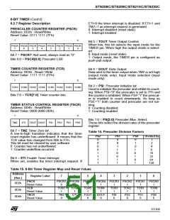
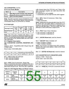
A/D CONVERTER CONTROL REGISTER (AD-
CR)
Note: This bit does not apply to the ADC peripher-
al but to the main clock system. Refer to the Clock
System section.
Address: 0D1h - Read/Write (Bit 6 Read Only, Bit
5 Write Only)
Reset value: 0100 0000 (40h)
7
0
Bits 1:0 = ADCR[1:0] Reserved, must be cleared.
ADCR OSC ADCR ADCR
EAI
EOC
STA
PDS
3
OFF
1
0
A/D CONVERTER DATA REGISTER (ADR)
Address: 0D0h - Read only
Bit 7 = EAI Enable A/D Interrupt.
0: ADC interrupt disabled
1: ADC interrupt enabled
Reset value: xxxx xxxx (xxh)
7
0
Bit 6 = EOC End of conversion. Read Only
ADR7 ADR6 ADR5 ADR4 ADR3 ADR2 ADR1 ADR0
When a conversion has been completed, this bit is
set by hardware and an interrupt request is gener-
ated if the EAI bit is set. The EOC bit is automati-
Bits 7:0 = ADR[7:0]: 8 Bit A/D Conversion Result.
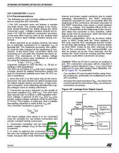
Table 16. ADC Register Map and Reset Values
Address
(Hex.)
Register
Label
7
6
5
4
3
2
1
0
ADR
Reset Value
ADR7
0
ADR6
0
ADR5
0
ADR4
0
ADR3
0
ADR2
0
ADR1
0
ADR0
0
0D0h
0D1h
ADCR
Reset Value
EAI
0
EOC
1
STA
0
PDS
0
ADCR3 OSCOFF ADCR1
ADCR0
0
0
0
0
55/104
1

 STMICROELECTRONICS [ ST ]