ST6208C/ST6209C/ST6210C/ST6220C
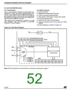
8.3 A/D CONVERTER (ADC)
8.3.1 Introduction
8.3.2 Main Features
■ 8-bit conversion
The on-chip Analog to Digital Converter (ADC) pe-
ripheral is a 8-bit, successive approximation con-
verter. This peripheral has multiplexed analog in-
put channels (refer to device pin out description)
that allow the peripheral to convert the analog volt-
age levels from different sources.
■ Multiplexed analog input channels
■ Linear successive approximation
■ Data register (DR) which contains the results
■ End of Conversion flag
■ On/Off bit (to reduce consumption)
The result of the conversion is stored in a 8-bit
Data Register. The A/D converter is controlled
through a Control Register.
■ Typical conversion time 70 µs (with an 8 MHz
crystal)
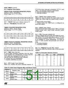
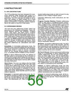
The block diagram is shown in Figure 34.
Figure 34. ADC Block Diagram
f
f
ADC
INT
DIV 12
AD AD
CR1 CR0
AD
CR3
OSC
OFF
EAI EOC STA PDS
ADCR
I/O PORT
AIN0
AIN1
ANALOG TO DIGITAL
CONVERTER
PORT
MUX
AINx
DDRx
ORx
ADR
DRx
ADR7 ADR6 ADR5 ADR4 ADR3 ADR2 ADR1 ADR0
Note: ADC not present on some devices. See device summary on page 1.
52/104
1

 STMICROELECTRONICS [ ST ]