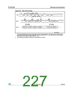
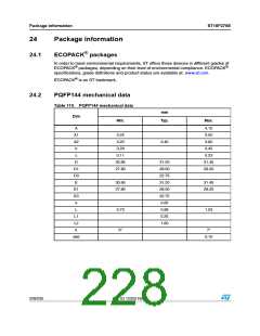
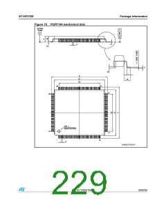
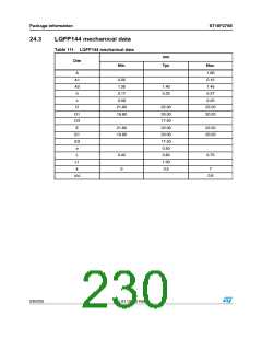
PDF
最近搜索
热门搜索
发布采购

| 型号: | ST10F276S-4T3 |
| PDF下载: | 下载PDF文件 查看货源 |
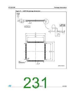
| 内容描述: | 16位MCU与MAC单元832 KB的闪存和68 KB的RAM [16-bit MCU with MAC unit 832 Kbyte Flash memory and 68 Kbyte RAM] |
| 分类和应用: | 闪存 |
| 文件页数/大小: | 235 页 / 2491 K |
| 品牌: |  STMICROELECTRONICS [ ST ] STMICROELECTRONICS [ ST ] |
专业IC领域供求交易平台:提供全面的IC Datasheet资料和资讯,Datasheet 1000万数据,IC品牌1000多家。