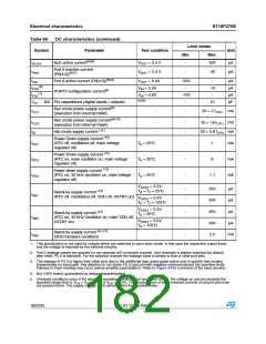
Electrical characteristics
ST10F276E
23
Electrical characteristics
23.1
Absolute maximum ratings
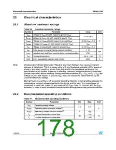
Table 86. Absolute maximum ratings
Symbol
Parameter
Value
Unit
VDD
Voltage on VDD pins with respect to ground (VSS)
- 0.3 to +6.5
VSTBY Voltage on VSTBY pin with respect to ground (VSS
VAREF Voltage on VAREF pin with respect to ground (VSS
VAGND Voltage on VAGND pin with respect to ground (VSS
)
)
- 0.3 to VDD + 0.3
V
)
VSS
- 0.5 to VDD + 0.5
10
VIO
IOV
Voltage on any pin with respect to ground (VSS
)
Input current on any pin during overload condition
mA
ITOV
TST
ESD
Absolute sum of all input currents during overload condition
Storage temperature
| 75 |
- 65 to +150
2000
°C
V
ESD susceptibility (human body model)
Note:
Stresses above those listed under “Absolute Maximum Ratings” may cause permanent
damage to the device. This is a stress rating only and functional operation of the device at
these or any other conditions above those indicated in the operational sections of this
specification is not implied. Exposure to absolute maximum rating conditions for extended
periods may affect device reliability. During overload conditions (VIN > VDD or VIN < VSS) the
voltage on pins with respect to ground (VSS) must not exceed the values defined by the
Absolute Maximum Ratings.
During Power-on and Power-off transients (including Stand-by entering/exiting phases), the
relationships between voltages applied to the device and the main VDD must always be
respected. In particular, power-on and power-off of VAREF must be coherent with the VDD
transient, in order to avoid undesired current injection through the on-chip protection diodes.
23.2
Recommended operating conditions
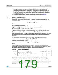
Table 87. Recommended operating conditions
Symbol
Parameter
Min.
Max.
Unit
VDD
VSTBY
VAREF
TA
Operating supply voltage
4.5
0
5.5
Operating stand-by supply voltage(1)
Operating analog reference voltage(2)
Ambient temperature under bias
Junction temperature under bias
V
VDD
+125
+150
-40
°C
TJ
178/235
Doc ID 12303 Rev 3

 STMICROELECTRONICS [ ST ]