SG2525A-SG3525A
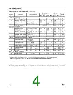
ELECTRICAL CHARACTERISTICS
(continued)
SG2525A
SG3525A
Symbol
Parameter
Test Conditions
Unit
Min. Typ. Max. Min. Typ. Max.
PWM COMPARATOR
Minimum Duty-cycle
0
0
%
%
V
•
•
Maximum Duty-cycle
Input Threshold
45
49
0.9
45
49
0.9
Zero Duty-cycle
0.7
0.7
Maximum Duty-cycle
3.3
3.6
1
3.3
3.6
1
V
*
Input Bias Current
0.05
0.05
µA
SHUTDOWN SECTION
Soft Start Current
VSD = 0 V, VSS = 0 V
VSD = 2.5 V
25
50
0.4
0.8
80
0.7
1
25
50
0.4
0.8
80
0.7
1
µA
V
Soft Start Low Level
Shutdown Threshold
To outputs, VSS = 5.1 V
0.6
0.6
V
Tj = 25 °C
Shutdown Input Current VSD = 2.5 V
Shutdown Delay VSD = 2.5 V Tj = 25 °C
OUTPUT DRIVERS (each output) (VC = 20 V)
0.4
0.2
1
0.4
0.2
1
mA
*
0.5
0.5
µs
Output Low Level
Isink = 20 mA
0.2
1
0.4
2
0.2
1
0.4
2
V
V
V
V
V
Isink = 100 mA
Isource = 20 mA
Isource = 100 mA
Output High Level
18
17
6
19
18
7
18
17
6
19
18
7
Under-Voltage Lockout Vcomp and Vss = High
8
8
IC
tr*
tf*
Collector Leakage
Rise Time
VC = 35 V
200
600
300
200
600
300
A
µ
CL = 1 nF, Tj = 25 °C
CL = 1 nF, Tj = 25 °C
100
50
100
50
ns
ns
Fall Time
TOTAL STANDBY CURRENT
Is Supply Current
Vi = 35 V
14
20
14
20
mA
*
•
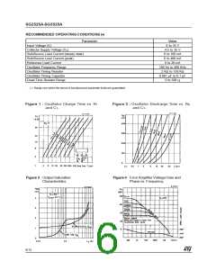
These parameters, although guaranteed over therecommended operating conditions, are not 100 % tested in production.
Tested at fosc = 40 KHz (RT = 3.6 KΩ, CT = 10nF, RD = 0 Ω). Approximate oscillator frequency is defined by :
1
f =
CT (0.7 RT + 3 RD)
DC transconductance (g ) relatesto DCopen-loop voltage gain(G ) according to thefollowing equation :G = gM RL whereRL isthe resistance
.
M
v
v
from pin 9 to ground. The minimum gM specification is used to calculate minimum Gv when the error amplifieroutput is loaded.
4/12

 STMICROELECTRONICS [ ST ]