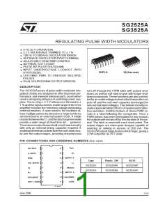
SG2525A-SG3525A
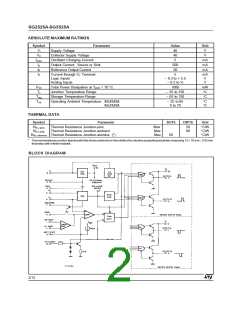
ABSOLUTE MAXIMUM RATINGS
Symbol
Parameter
Value
40
Unit
V
Vi
VC
IOSC
Io
Supply Voltage
Collector Supply Voltage
Oscillator Charging Current
40
V
5
mA
mA
mA
Output Current, Source or Sink
Reference Output Current
500
50
IR
IT
Current through CT Terminal
Logic Inputs
Analog Inputs
5
mA
V
V
– 0.3 to + 5.5
– 0.3 to Vi
Ptot
Tj
Total Power Dissipation at Tamb = 70 °C
Junction Temperature Range
1000
mW
– 55 to 150
– 65 to 150
C
°
Tstg
Top
Storage Temperature Range
C
°
Operating Ambient Temperature : SG2525A
– 25 to 85
0 to 70
C
°
°C
SG3525A
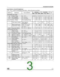
THERMAL DATA
Symbol
Parameter
Thermal Resistance Junction-pins
Thermal Resistance Junction-ambient
SO16
DIP16
Unit
Rth j-pins
Rth j-amb
Max
Max
Max
50
80
°C/W
C/W
°
Rth j-alumina Thermal Resistance Junction-alumina (*)
50
°C/W
*
Thermalresistance junction-aluminawiththe devicesoldered on themiddleofan aluminasupportingsubstrate measuring 15× 20mm; 0.65mm
thickness with infiniteheatsink.
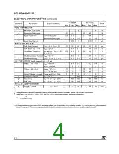
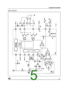
BLOCK DIAGRAM
2/12

 STMICROELECTRONICS [ ST ]