L7250
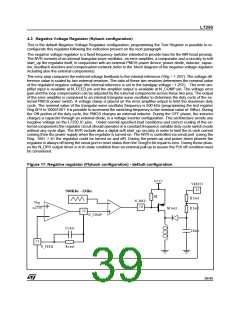
4.3 Negative Voltage Regulator (flyback configuration)
This is the default Negative Voltage Regulator configuration; programming the Test Register is possible to re-
configurate this regulator following the indication present on the next paragraph.
The negative voltage regulator is a fixed frequency switcher intended to provide bias for the MR head preamp.
The NVR consists of an internal triangular wave oscillator, an error amplifier, a comparator and a circuitry to soft
start_up the regulator itself, in conjunction with an external PMOS power device, power diode, inductor, capac-
itor, feedback resistors and compensation network (refer to the block diagram of the negative voltage regulator
including also the external components).
The error amp compares the external voltage feedback to the internal reference (Vbg = 1.25V). The voltage dif-
ference value is scaled by two external resistors. The ratio of these two resistors determines the nominal value
of the regulated negative voltage (the internal reference is set to the bandgap voltage ~1.25V). The error am-
plifier input is available at N_FEED pin and the amplifier output is available at N_COMP pin. The voltage error
gain and the loop compensation can be adjusted by the external components across these two pins. The output
of the error amplifier is compared to an internal triangular wave oscillator to determine the duty cycle of the ex-
ternal PMOS power switch. A voltage clamp is placed on the error amplifier output to limit the maximum duty
cycle. The nominal value of the triangular wave oscillator frequency is 500 kHz (programming the test register
Reg 0FH to ‘00001001’ it is possible to increment the switching frequency to the nominal value of 1Mhz). During
the ON portion of the duty cycle, the PMOS charges an external inductor. During the OFF phase, the inductor
charges a capacitor through an external diode, in a voltage inverter configuration. This architecture avoids any
negative voltage on the L7250 IC pins. Under normal specified load conditions and correct scaling of the ex-
ternal components the regulator circuit should operates in a constant frequency variable duty cycle switch mode
without any cycle slips. The NVR include also a digital soft start_up circuitry in order to limit the in rush current
coming from the power supply when the regulator is turned-on. The NVR is controlled via serial port (using the
Reg. 05H -> b1 the regulator could be turned on and off). During the power-up and power-down phases the
regulator is always off being the serial port in reset status then the VnegEn bit equal to zero. During those phas-
es the N_DRV output driver is in tri-state condition then an external pull-up to assure the Pch off condition must
be considered.
Figure 17. Negative regulator (Flyback configuration) - default configuration
V C C 5
V R E F2 5
21
500Khz - 1Mhz
5K
R 1ext
N _D R V
V b g
10
(typ 1.2 5)
M 1ext
R 2ext
C fext
12
N _ C O M P
C cext
R cext
11
N _FE E D
39/46

 STMICROELECTRONICS [ ST ]