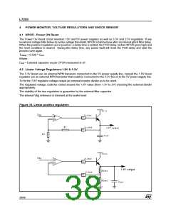
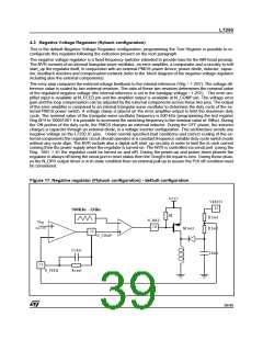
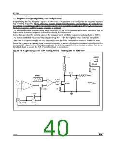
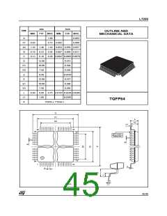
L7250
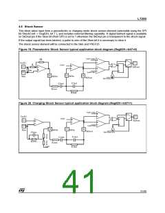
4.5 Shock Sensor
This block takes input from a piezoelectric or charging mode shock sensor element (selectable using the SPI
bit ShockConf -> Reg02H, bit 7 ), and includes external filtering capability. A digital latched signal is available
on SkDout pin if the Sken bit (from SPI) is set to 1 otherwise the SkDout pin is transparent to the shock signal.
If the output signal has been latched, a pulse to zero of the Sken bit it is necessary to clear it.
The shock sensor element will be connected to the Skin and VREF25.
Figure 19. Piezoelectric Shock Sensor typical application block diagram (Reg02H->bit7=0)
Vref25+VthH
9 R
0
V re f25
2 1
2 7
R
Vref25
1
S
S k D ou t
10M
R
Vref25-VthL
S k F ou t
2 3
25
24
2 6
S k F in
S k in
S k O u t
R 1ext
SkEn (from SPI)
C 2ex t
C 1ex t
R 2 ext
Figure 20. Charging Shock Sensor typical application block diagram (Reg02H->bit7=1)
V ref25+V thH
0
V re f2 5
2 7
1
Vref25
S
2 1
S kD o u t
R
Vref25-VthL
S k F o u t
2 3
25
24
2 6
S k F in
S k in
S k O u t
R 1ex t
SkEn (from SPI)
C S ext
R S ext
C 2 ext
C 1 ext
V ref25
R 2ext
41/46

 STMICROELECTRONICS [ ST ]