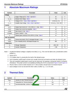
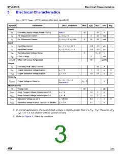
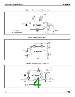
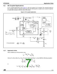
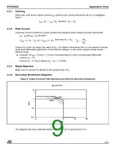
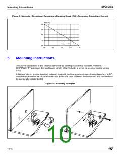
Application Hints
4.1.1.1 Centering
STV9302A
Display will be centered (null mean current in yoke) when voltage on pin 7 is (R is negligible):
1
V
+ V
R
ꢀ
ꢀ
ÿ
ꢀ
2
M
m
------------------------
---------------------
ꢀ
V
=
×
7
2
R + R
þ
3
2
4.1.1.2 Peak Current
(V – V
)
R
M
m
2
I
=
×
---------------------------- ------------------
P
2
R xR
1
3
Example: for V = 2 V, V = 5 V and I = 1 A
m
M
P
Choose R in the1 Ω range, for instance R =1 Ω
1
1
2 × I × R
R
P
1
2
2
3
From equation of peak current:
-----------------------------
------- =
= --
V
– V
R
3
M
m
Then choose R or R . For instance, if R = 10 kΩ, then R = 15 kΩ
2
3
2
3
Finally, the bias voltage on pin 7 should be:
+ V
V
M
m
1
R
7
2
1
2.5
V
=
×
=
×
= 1.4V
------------------------ ----------------- -- -------
7
2
3
1 + -------
R
2
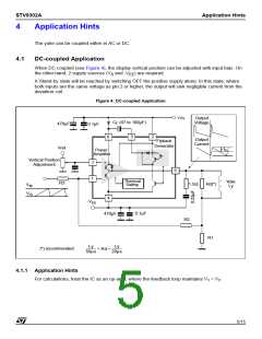
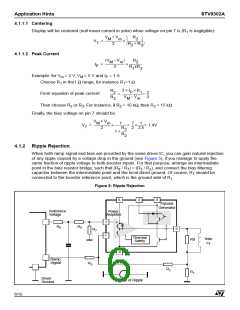
4.1.2 Ripple Rejection
When both ramp signal and bias are provided by the same driver IC, you can gain natural rejection
of any ripple caused by a voltage drop in the ground (see Figure 5), if you manage to apply the
same fraction of ripple voltage to both booster inputs. For that purpose, arrange an intermediate
point in the bias resistor bridge, such that (R / R ) = (R / R ), and connect the bias filtering
8
7
3
2
capacitor between the intermediate point and the local driver ground. Of course, R should be
7
connected to the booster reference point, which is the ground side of R .
1
Figure 5: Ripple Rejection
3
2
6
Flyback
Generator
Reference
Voltage
Power
Amplifier
7
+
R9
R8
5
R7
1
-
Thermal
Safety
Yoke
Ly
Rd
4
Ramp
Signal
R3
R2
R1
Driver
Ground
Source of Ripple
6/15

 STMICROELECTRONICS [ ST ]