STV9302A
Application Hints
4.3.1 Centring
When idle, both driver outputs provide i and the yoke current should be null (R is negligible),
cm
1
hence:
i
R
= i
R
therefore R = R
cm
7
cm
2
7
2
4.3.2 Peak Current
Scanning current should be I when positive and negative driver outputs provide respectively
P
i
- i and i + i , therefore
p cm p
cm
I
2R
and since R = R :
7
2
(i
– i) R = I R + (i
+ i) R
p
i
7
cm
7
p
1
cm
2
---- = –
----------
R
1
Choose R in the 1Ω range, the value of R = R follows. Remember that i is one-quarter of driver
1
2
7
peak-peak differential signal! Also check that the voltages on the driver outputs remain inside
allowed range.
● Example: for i = 0.4mA, i = 0.2mA (corresponding to 0.8mA of peak-peak differential
cm
current), I = 1A
p
Choose R = 0.75Ω, it follows R = R = 1.875kΩ.
1
2
7
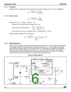
4.3.3 Ripple Rejection
Make sure to connect R directly to the ground side of R .
7
1
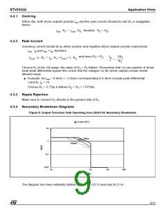
4.3.4 Secondary Breakdown Diagrams
Figure 8: Output Transistor Safe Operating Area (SOA) for Secondary Breakdown
@ Tcase=25°C
10
100µs
10ms
1
100ms
0.1
0.01
10
35
60
100
Volts
The diagram has been arbitrarily limited to max VS (35 V) and max I0 (2 A).
9/15

 STMICROELECTRONICS [ ST ]