Absolute Maximum Ratings
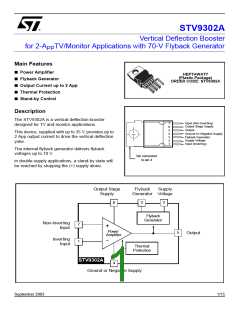
STV9302A
1
Absolute Maximum Ratings
Symbol
Voltage
Parameter
Value
Unit
VS
V5, V6
V3
Supply Voltage (pin 2) - Note 1 and Note 2
Flyback Peak Voltage - Note 2
40
70
V
V
V
Voltage at Pin 3 - Note 2, Note 3 and Note 6
Amplifier Input Voltage - Note 2, Note 6 and Note 7
-0.4 to (VS + 3)
V1, V7
- 0.4 to (VS + 2) or +40
V
Current
I0 (1)
I0 (2)
Output Peak Current at f = 50 to 200 Hz, t ≤ 10µs - Note 4
Output Peak Current non-repetitive - Note 5
Sink Current, t<1ms - Note 3
±5
±2
A
A
A
A
A
I3 Sink
I3 Source
I3
1.5
1.5
±5
Source Current, t < 1ms
Flyback pulse current at f=50 to 200 Hz, t≤10µs - Note 4
ESD Susceptibility
ESD1
ESD2
Human body model (100 pF discharged through 1.5 kΩ)
EIAJ Standard (200 pF discharged through 0 Ω)
2
kV
V
300
Temperature
Ts
Storage Temperature
Junction Temperature
-40 to 150
+150
°C
°C
Tj
Note:1. Usually the flyback voltage is slightly more than 2 x V . This must be taken into consideration when
S
setting V
S.
2. Versus pin 4
3. V3 is higher than V during the first half of the flyback pulse.
S
4. Such repetitive output peak currents are usually observed just before and after the flyback pulse.
5. This non-repetitive output peak current can be observed, for example, during the Switch-On/Switch-
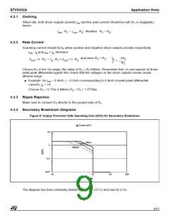
Off phases. This peak current is acceptable providing the SOA is respected (Figure 8 and Figure 9).
6. All pins have a reverse diode towards pin 4, these diodes should never be forward-biased.
7. Input voltages must not exceed the lower value of either V + 2 or 40 volts.
S
2
Thermal Data
Symbol
RthJC
TT
Parameter
Junction-to-Case Thermal Resistance
Temperature for Thermal Shutdown
Recommended Max. Junction Temperature
Value
3
Unit
°C/W
°C
150
120
TJ
°C
2/15

 STMICROELECTRONICS [ ST ]