FlashFlex MCU
SST89E564RD / SST89V564RD
SST89E554RC / SST89V554RC
EOL Data Sheet
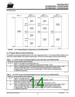
EA# = 1
SFCF[1:0] = 00
EA# = 1
SFCF[1:0] = 01
EA# = 1
SFCF[1:0] = 10, 11
EA# = 0
FFFFH
FFFFH
FFFFH
FFFFH
8 KByte
Block 1
8 KByte
Block 1
E000H
DFFFH
E000H
DFFFH
External
32 KByte
External
24 KByte
External
24 KByte
External
64 KByte
8000H
7FFFH
8000H
7FFFH
8000H
7FFFH
24 KByte
Block 0
2000H
1FFFH
32 KByte
Block 0
32 KByte
Block 0
8 KByte
Block 1
0000H
0000H
0000H
0000H
1207 F03.2
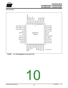
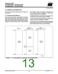
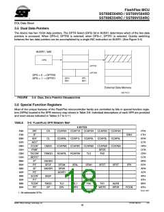
FIGURE
3-2: PROGRAM MEMORY ORGANIZATION FOR SST89E/V554RC
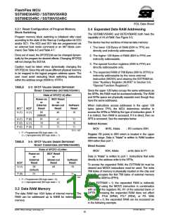
3.2 Program Memory Block Switching
The program memory block switching feature of the device allows either Block 1 or the lowest 8 KByte of Block 0 to be
used for the lowest 8 KByte of the program address space. SFCF[1:0] controls program memory block switching.
TABLE
SFCF[1:0]
01, 10, 11
3-1: SFCF VALUES FOR PROGRAM MEMORY BLOCK SWITCHING FOR SST89E/V564RD
Program Memory Block Switching
Block 1 is not visible to the program counter (PC).
Block 1 is reachable only via in-application programming from 0000H - 1FFFH.
00
Block 1 is overlaid onto the low 8K of the program address space; occupying address locations 0000H - 1FFFH.
When the PC falls within 0000H - 1FFFH, the instruction will be fetched from Block 1 instead of Block 0.
Outside of 0000H - 1FFFH, Block 0 is used. Locations 0000H - 1FFFH of Block 0 are reachable through
in-application programming.
T3-1.1 1207
TABLE
3-2: SFCF VALUES FOR PROGRAM MEMORY BLOCK SWITCHING FOR SST89E/V554RC
SFCF[1:0]
Program Memory Block Switching
10, 11
Block 1 is not visible to the PC;
Block 1 is reachable only via in-application programming from E000H - FFFFH.
01
00
Both Block 0 and Block 1 are visible to the PC.
Block 0 is occupied from 0000H - 7FFFH. Block 1 is occupied from E000H - FFFFH.
Block 1 is overlaid onto the low 8K of the program address space; occupying address locations 0000H - 1FFFH.
When the PC falls within 0000H - 1FFFH, the instruction will be fetched from Block 1 instead of Block 0.
Outside of 0000H - 1FFFH, Block 0 is used. Locations 0000H - 1FFFH of Block 0 are reachable through
in-application programming.
T3-2.0 1207
©2007 Silicon Storage Technology, Inc.
S71207-08-EOL
1/07
14

 SST [ SILICON STORAGE TECHNOLOGY, INC ]