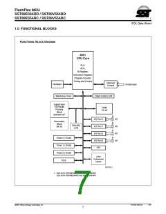
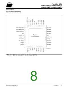
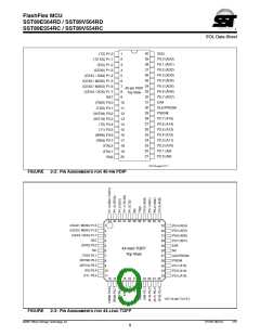
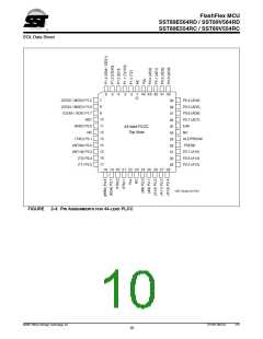
FlashFlex MCU
SST89E564RD / SST89V564RD
SST89E554RC / SST89V554RC
EOL Data Sheet
2.1 Pin Descriptions
TABLE
Symbol
2-1: PIN DESCRIPTIONS (1 OF 2)
Type1
Name and Functions
P0[7:0]
I/O
Port 0: Port 0 is an 8-bit open drain bi-directional I/O port. As an output port each pin can
sink several LS TTL inputs. Port 0 pins that have ‘1’s written to them float, and in this state
can be used as high-impedance inputs. Port 0 is also the multiplexed low-order address and
data bus during accesses to external code and data memory. In this application, it uses
strong internal pull-ups when transitioning to ‘1’s. Port 0 also receives the code bytes during
the external host mode programming, and outputs the code bytes during the external host
mode verification. External pull-ups are required during program verification or as a general
purpose I/O port.
P1[7:0]
I/O with internal Port 1: Port 1 is an 8-bit bi-directional I/O port with internal pull-ups. The Port 1 output buffers
pull-up
can drive LS TTL inputs. Port 1 pins are pulled high by the internal pull-ups when ‘1’s are writ-
ten to them and can be used as inputs in this state. As inputs, Port 1 pins that are externally
pulled low will source current (IIL, see Tables 13-6 and 13-7) because of the internal pull-ups.
P1[5, 6, 7] have high current drive of 16 mA. Port 1 also receives the low-order address bytes
during the external host mode programming and verification.
P1[0]
P1[1]
P1[2]
I/O
T2: External count input to Timer/Counter 2 or Clock-out from Timer/Counter 2
T2EX: Timer/Counter 2 capture/reload trigger and direction control
I
I
ECI: External Clock Input
This signal is the external clock input for the PCA.
P1[3]
P1[4]
P1[5]
P1[6]
P1[7]
P2[7:0]
I/O
I/O
I/O
I/O
I/O
CEX0: Capture/Compare External I/O for PCA Module 0
Each capture/compare module connects to a Port 1 pin for external I/O.
When not used by the PCA, this pin can handle standard I/O.
SS#: Slave port select input for SPI
OR
CEX1: Capture/Compare External I/O for PCA Module 1
MOSI: Master Output line, Slave Input line for SPI
OR
CEX2: Capture/Compare External I/O for PCA Module 2
MISO: Master Input line, Slave Output line for SPI
OR
CEX3: Capture/Compare External I/O for PCA Module 3
SCK: Master clock output, slave clock input line for SPI
OR
CEX4: Capture/Compare External I/O for PCA Module 4
I/O
Port 2: Port 2 is an 8-bit bi-directional I/O port with internal pull-ups. Port 2 pins are pulled
high by the internal pull-ups when ‘1’s are written to them and can be used as inputs in this
state. As inputs, Port 2 pins that are externally pulled low will source current (IIL, see Tables
13-6 and 13-7) because of the internal pull-ups. Port 2 sends the high-order address byte
during fetches from external program memory and during accesses to external Data Memory
that use 16-bit address (MOVX@DPTR). In this application, it uses strong internal pull-ups
when transitioning to ‘1’s. Port 2 also receives some control signals and a partial of high-order
address bits during the external host mode programming and verification.
with internal
pull-up
P3[7:0]
I/O
Port 3: Port 3 is an 8-bit bidirectional I/O port with internal pull-ups. The Port 3 output buffers
can drive LS TTL inputs. Port 3 pins are pulled high by the internal pull-ups when ‘1’s are writ-
ten to them and can be used as inputs in this state. As inputs, Port 3 pins that are externally
pulled low will source current (IIL, see Tables 13-6 and 13-7) because of the internal pull-ups.
Port 3 also receives some control signals and a partial of high-order address bits during the
external host mode programming and verification.
with internal
pull-up
P3[0]
P3[1]
I
RXD: Universal Asynchronous Receiver/Transmitter (UART) - Receive input
TXD: UART - Transmit output
O
©2007 Silicon Storage Technology, Inc.
S71207-08-EOL
1/07
11

 SST [ SILICON STORAGE TECHNOLOGY, INC ]