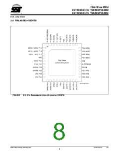
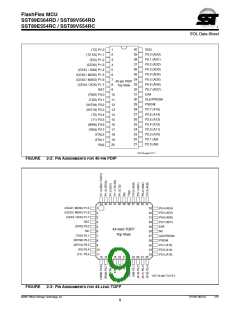
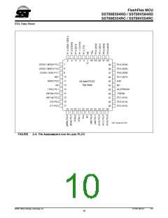
FlashFlex MCU
SST89E564RD / SST89V564RD
SST89E554RC / SST89V554RC
EOL Data Sheet
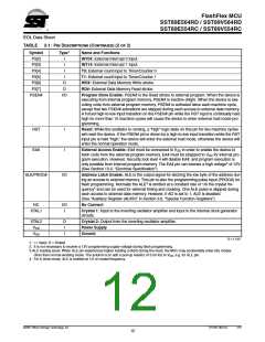
TABLE
Symbol
2-1: PIN DESCRIPTIONS (CONTINUED) (2 OF 2)
Type1
Name and Functions
P3[2]
P3[3]
P3[4]
P3[5]
P3[6]
P3[7]
PSEN#
I
I
INT0#: External Interrupt 0 Input
INT1#: External Interrupt 1 Input
I
T0: External count input to Timer/Counter 0
T1: External count input to Timer/Counter 1
WR#: External Data Memory Write strobe
RD#: External Data Memory Read strobe
I
O
O
I/O
Program Store Enable: PSEN# is the Read strobe to external program. When the device is
executing from internal program memory, PSEN# is inactive (High). When the device is exe-
cuting code from external program memory, PSEN# is activated twice each machine cycle,
except that two PSEN# activations are skipped during each access to external data memory.
A forced high-to-low input transition on the PSEN# pin while the RST input is continually held
high for more than 10 machine cycles will cause the device to enter external host mode pro-
gramming.
RST
EA#
I
I
Reset: While the oscillator is running, a “high” logic state on this pin for two machine cycles
will reset the device. If the PSEN# pin is driven by a high-to-low input transition while the RST
input pin is held “high,” the device will enter the external host mode, otherwise the device will
enter the normal operation mode.
External Access Enable: EA# must be connected to VSS in order to enable the device to
fetch code from the external program memory. EA# must be strapped to VDD for internal pro-
gram execution. However, Security lock level 4 will disable EA#, and program execution is
only possible from internal program memory. The EA# pin can tolerate a high voltage2 of 12V.
(See Section 13.0, “Electrical Specification”)
ALE/PROG#
I/O
Address Latch Enable: ALE is the output signal for latching the low byte of the address dur-
ing an access to external memory. This pin is also the programming pulse input (PROG#) for
flash programming. Normally the ALE3 is emitted at a constant rate of 1/6 the crystal fre-
quency4 and can be used for external timing and clocking. One ALE pulse is skipped during
each access to external data memory. However, if AO is set to 1, ALE is disabled.
(See “Auxiliary Register (AUXR)” in Section 3.6, “Special Function Registers”)
NC
I/O
I
No Connect
XTAL1
Crystal 1: Input to the inverting oscillator amplifier and input to the internal clock generator
circuits.
XTAL2
VDD
O
I
Crystal 2: Output from the inverting oscillator amplifier.
Power Supply
VSS
I
Ground
T2-1.4 1207
1. I = Input; O = Output
2. It is not necessary to receive a 12V programming supply voltage during flash programming.
3.ALE loading issue: When ALE pin experiences higher loading (>30pf) during the reset, the MCU may accidentally enter into modes
other than normal working mode. The solution is to add a pull-up resistor of 3-50 KΩ to VDD, e.g. for ALE pin.
4. For 6 clock mode, ALE is emitted at 1/3 of crystal frequency.
©2007 Silicon Storage Technology, Inc.
S71207-08-EOL
1/07
12

 SST [ SILICON STORAGE TECHNOLOGY, INC ]