FlashFlex MCU
SST89E564RD / SST89V564RD
SST89E554RC / SST89V554RC
EOL Data Sheet
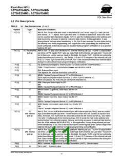
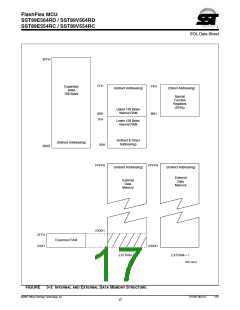
3.0 MEMORY ORGANIZATION
The device has separate address spaces for program and
data memory.
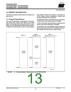
bank selection. Please refer to Figure 3-1 and Figure 3-2
for the program memory configurations. Program bank
selection is described in the next section.
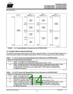
3.1 Program Flash Memory
The 64K/32K x8 primary SuperFlash block is organized as
512/256 sectors, each sector consists of 128 Bytes.
There are two internal flash memory blocks in the device.
The primary flash memory block (Block 0) has 64/32
KByte. The secondary flash memory block (Block 1) has 8
KByte. Since the total program address space is limited to
64 KByte, the SFCF[1:0] bit are used to control program
The 8K x8 secondary SuperFlash block is organized as 64
sectors, each sector consists also of 128 Bytes.
For both blocks, the 7 least significant program address bits
select the byte within the sector. The remainder of the pro-
gram address bits select the sector within the block.
EA# = 1
SFCF[1:0] = 00
EA# = 1
SFCF[1:0] = 01, 10, 11
EA# = 0
FFFFH
FFFFH
FFFFH
56 KByte
Block 0
64 KByte
Block 0
External
64 KByte
2000H
1FFFH
8 KByte
Block 1
0000H
0000H
0000H
1207 F02.0
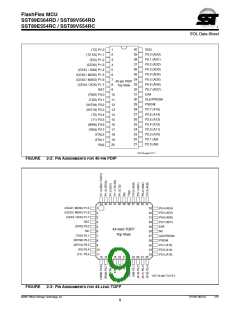
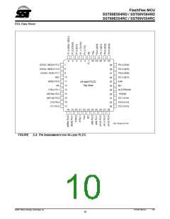
FIGURE
3-1: PROGRAM MEMORY ORGANIZATION FOR SST89E/V564RD
©2007 Silicon Storage Technology, Inc.
S71207-08-EOL
1/07
13

 SST [ SILICON STORAGE TECHNOLOGY, INC ]