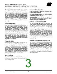
8 Mbit / 16 Mbit Multi-Purpose Flash
SST39LF080 / SST39LF016 / SST39VF080 / SST39VF016
Data Sheet
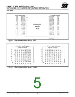
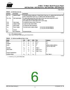
TABLE 2: PIN DESCRIPTION
Symbol
Pin Name
Functions
AMS1-A0
Address Inputs
To provide memory addresses. During Sector-Erase AMS-A12 address lines will select the
sector. During Block-Erase AMS-A16 address lines will select the block.
DQ7-DQ0
Data Input/output
To output data during Read cycles and receive input data during Write cycles.
Data is internally latched during a Write cycle.
The outputs are in tri-state when OE# or CE# is high.
CE#
OE#
WE#
VDD
Chip Enable
Output Enable
Write Enable
Power Supply
To activate the device when CE# is low.
To gate the data output buffers.
To control the Write operations.
To provide power supply voltage:
3.0-3.6V for SST39LF080/016
2.7-3.6V for SST39VF080/016
VSS
NC
Ground
No Connection
Unconnected pins.
T2.3 396
1. AMS = Most significant address
MS = A19 for SST39LF/VF080 and A20 for SST39LF/VF016
A
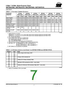
TABLE 3: OPERATION MODES SELECTION
Mode
Read
CE#
VIL
OE#
VIL
WE#
VIH
VIL
DQ
DOUT
DIN
X1
Address
AIN
Program
Erase
VIL
VIH
VIH
AIN
VIL
VIL
Sector or Block address,
XXH for Chip-Erase
Standby
VIH
X
X
VIL
X
X
X
High Z
X
X
X
Write Inhibit
High Z/ DOUT
High Z/ DOUT
X
VIH
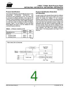
Product Identification
Software Mode
VIL
VIL
VIH
See Table 4
T3.4 396
1. X can be VIL or VIH, but no other value.
©2001 Silicon Storage Technology, Inc.
S71146-03-000 6/01 396
6

 SST [ SILICON STORAGE TECHNOLOGY, INC ]