8 Mbit / 16 Mbit Multi-Purpose Flash
SST39LF080 / SST39LF016 / SST39VF080 / SST39VF016
Data Sheet
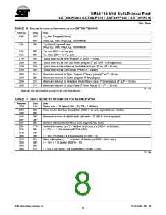
TABLE 6: SYSTEM INTERFACE INFORMATION FOR SST39VF320/640
Address
Data
27H1
30H1
36H
Data
1BH
VDD Min (Program/Erase)
DQ7-DQ4: Volts, DQ3-DQ0: 100 millivolts
1CH
VDD Max (Program/Erase)
DQ7-DQ4: Volts, DQ3-DQ0: 100 millivolts
1DH
1EH
1FH
20H
21H
22H
23H
24H
25H
26H
00H
00H
04H
00H
04H
06H
01H
00H
01H
01H
VPP min. (00H = no VPP pin)
VPP max. (00H = no VPP pin)
Typical time out for Byte-Program 2N µs (24 = 16 µs)
Typical time out for min. size buffer program 2N µs (00H = not supported)
Typical time out for individual Sector/Block-Erase 2N ms (24 = 16 ms)
Typical time out for Chip-Erase 2N ms (26 = 64 ms)
Maximum time out for Byte-Program 2N times typical (21 x 24 = 32 µs)
Maximum time out for buffer program 2N times typical
Maximum time out for individual Sector/Block-Erase 2N times typical (21 x 24 = 32 ms)
Maximum time out for Chip-Erase 2N times typical (21 x 26 = 128 ms)
T6.1 396
1. 0030H for SST39LF080/016 and 0027H for SST39VF080/016
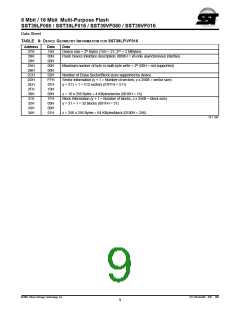
TABLE 7: DEVICE GEOMETRY INFORMATION FOR SST39LF/VF080
Address
27H
28H
Data
14H
00H
00H
00H
00H
02H
FFH
00H
10H
00H
0FH
00H
00H
01H
Data
Device size = 2N Bytes (14H = 20; 220 = 1 MBytes)
Flash Device Interface description; 0000H = x8-only asynchronous interface
29H
2AH
2BH
2CH
2DH
2EH
2FH
30H
31H
32H
33H
34H
Maximum number of byte in multi-byte write = 2N (00H = not supported)
Number of Erase Sector/Block sizes supported by device
Sector Information (y + 1 = Number of sectors; z x 256B = sector size)
y = 255 + 1 = 256 sectors (00FFH = 255)
z = 16 x 256 Bytes = 4 KBytes/sector (0010H = 16)
Block Information (y + 1 = Number of blocks; z x 256B = block size)
y = 15 + 1 = 16 blocks (000FH = 15)
z = 256 x 256 Bytes = 64 KBytes/block (0100H = 256)
T7.0 396
©2001 Silicon Storage Technology, Inc.
S71146-03-000 6/01 396
8

 SST [ SILICON STORAGE TECHNOLOGY, INC ]